. 2001 Apr 24;98(9):4835-40.
doi: 10.1073/pnas.091588098.

Paper-like electronic displays: large-area rubber-stamped plastic sheets of electronics and microencapsulated electrophoretic inks

Affiliations

Paper-like electronic displays: large-area rubber-stamped plastic sheets of electronics and microencapsulated electrophoretic inks

J A Rogers et al. Proc Natl Acad Sci U S A. .

Abstract

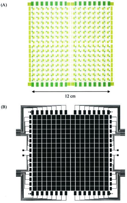
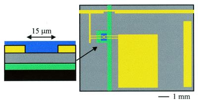
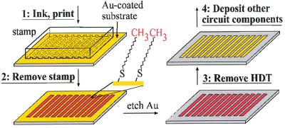
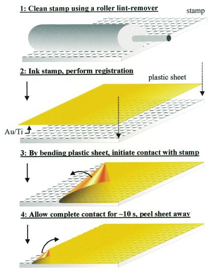
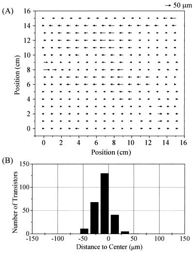
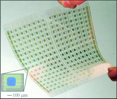
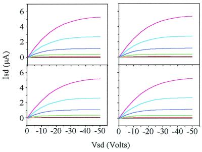
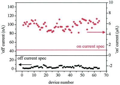
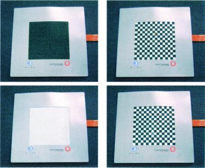
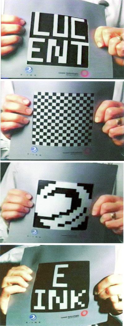
Electronic systems that use rugged lightweight plastics potentially offer attractive characteristics (low-cost processing, mechanical flexibility, large area coverage, etc.) that are not easily achieved with established silicon technologies. This paper summarizes work that demonstrates many of these characteristics in a realistic system: organic active matrix backplane circuits (256 transistors) for large ( approximately 5 x 5-inch) mechanically flexible sheets of electronic paper, an emerging type of display. The success of this effort relies on new or improved processing techniques and materials for plastic electronics, including methods for (i) rubber stamping (microcontact printing) high-resolution ( approximately 1 microm) circuits with low levels of defects and good registration over large areas, (ii) achieving low leakage with thin dielectrics deposited onto surfaces with relief, (iii) constructing high-performance organic transistors with bottom contact geometries, (iv) encapsulating these transistors, (v) depositing, in a repeatable way, organic semiconductors with uniform electrical characteristics over large areas, and (vi) low-temperature ( approximately 100 degrees C) annealing to increase the on/off ratios of the transistors and to improve the uniformity of their characteristics. The sophistication and flexibility of the patterning procedures, high level of integration on plastic substrates, large area coverage, and good performance of the transistors are all important features of this work. We successfully integrate these circuits with microencapsulated electrophoretic "inks" to form sheets of electronic paper.


Figures

Figure 1
Figure 1
(A) Layout of gate (green) and source/drain (yellow) levels of an active matrix backplane circuit for a sheet of electronic paper with 256 pixels. (B) Layout of pixel electrodes and pinout connections. The electrodes in B are bonded to a sheet that connects to the electronic ink on one side and to the backplane circuit on the other.
Figure 2
Figure 2
Schematic illustration of the cross section of a display transistor and layout of a unit cell (blue, semiconductor; yellow, gold source/drain level; gray, dielectric; green, gate level; black, substrate). Each transistor controls the switching of electronic ink that lies above a pixel electrode that is electrically connected to the drain side of the transistor. The rectangle of gold on the right is generated by a raised support feature on the stamp that prevents mechanical sagging in the recessed regions during printing.
Figure 3
Figure 3
Procedures for μCP source/drain electrodes for bottom contact organic transistors. Using a rubber stamp to print an ink of hexadecanethiol (HDT) yields a patterned SAM in the geometry of the stamp. Etching the gold that is not protected by the SAM produces a conducting circuit pattern. Removing the SAM facilitates electrical contact between these patterns and layers of organic semiconductor deposited on top of them.
Figure 4
Figure 4
Procedures for using μCP to pattern over large areas, with low defects, low distortions, and good registration to existing features. The stamp is first placed, printing side up, on a surface that allows strains in the stamp to relax; the stamp is never directly manipulated again. A conventional roller lint remover removes dust from the surface of the stamp. After inking, registration marks on the plastic substrate are aligned with similar marks on the stamp. By gradually unbending the substrate, contact proceeds from the registered edge to the other in a manner that minimizes the formation of trapped pockets of air. Peeling the plastic sheet away from the stamp after maintaining contact for ≈10 s completes the printing.
Figure 5
Figure 5
Registration errors in a typical printed circuit, measured by using a microscope to examine the relative positions of features in the source/drain and gate levels. The results define variations in the lateral distance between the center of each transistor channel and the midpoint between the edges of the gate pad that lie parallel to the channel width. Both the overall positioning accuracy and the distortions easily meet the requirements for this application.
Figure 6
Figure 6
Image of a completed plastic active matrix backplane circuit. The Inset shows an optical micrograph of a typical transistor.
Figure 7
Figure 7
Current–voltage characteristics of several typical transistors in a rubber-stamped plastic backplane circuit. In each case, the gate voltage varied from 0 V to −50 V in steps of −10 V.
Figure 8
Figure 8
On and off currents measured from 64 transistors in a printed backplane circuit. In all cases, the currents meet the required specifications. The on current is measured with Vsd = −50 V and Vg = −50 V. The off current is measured with Vsd = −50 V and Vg = 0 V. Leakage currents measured with Vsd = 0V and Vg = −50 V (not shown here) have magnitudes similar to the off currents.
Figure 9
Figure 9
Sheet of electronic paper (total thickness, ≈1 mm) displaying several different images. The time for the display to switch from one image to another is ≈1 s.
Figure 10
Figure 10
Sheet of electronic paper displaying images while being mechanically flexed. Bending does not alter the performance of the display.

Comment in

References

    1. Ota I, Ohnishi J, Yoshiyama M. Proc IEEE. 1973;61:832–836.
    1. Comiskey B, Albert J D, Yoshizawa H, Jacobson J. Nature (London) 1998;394:253–255.
    1. Hebner T R, Wu C C, Marcy D, Lu M H, Sturm J C. Appl Phys Lett. 1998;72:519–521.
    1. Chang S C, Bharathan J, Yang Y, Helgeson R, Wudl F, Ramey M B, Reynolds J R. Appl Phys Lett. 1998;73:2561–2563.
    1. Bao Z, Feng Y, Dodabalapur A, Raju V R, Lovinger A J. Chem Mater. 1997;9:1299–1301.

LinkOut - more resources