

Viral assembly of oriented quantum dot nanowires
- PMID: 12777631
- PMCID: PMC165810
- DOI: 10.1073/pnas.0832310100
Viral assembly of oriented quantum dot nanowires
Abstract
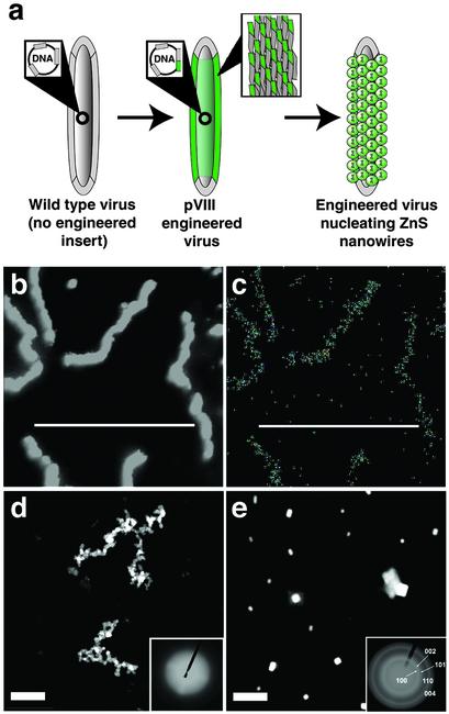
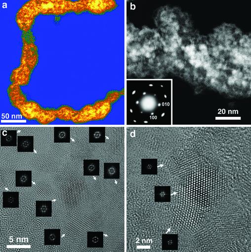
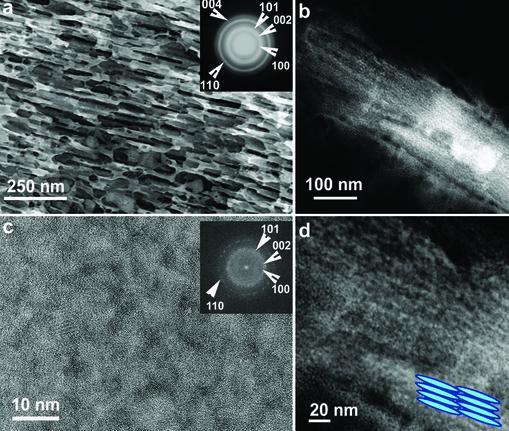
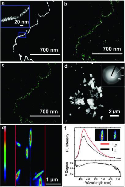
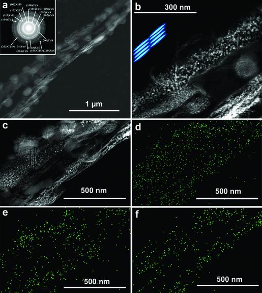
The highly organized structure of M13 bacteriophage was used as an evolved biological template for the nucleation and orientation of semiconductor nanowires. To create this organized template, peptides were selected by using a pIII phage display library for their ability to nucleate ZnS or CdS nanocrystals. The successful peptides were expressed as pVIII fusion proteins into the crystalline capsid of the virus. The engineered viruses were exposed to semiconductor precursor solutions, and the resultant nanocrystals that were templated along the viruses to form nanowires were extensively characterized by using high-resolution analytical electron microscopy and photoluminescence. ZnS nanocrystals were well crystallized on the viral capsid in a hexagonal wurtzite or a cubic zinc blende structure, depending on the peptide expressed on the viral capsid. Electron diffraction patterns showed single-crystal type behavior from a polynanocrystalline area of the nanowire formed, suggesting that the nanocrystals on the virus were preferentially oriented with their [001] perpendicular to the viral surface. Peptides that specifically directed CdS nanocrystal growth were also engineered into the viral capsid to create wurtzite CdS virus-based nanowires. Lastly, heterostructured nucleation was achieved with a dual-peptide virus engineered to express two distinct peptides within the same viral capsid. This work represents a genetically controlled biological synthesis route to a semiconductor nanoscale heterostructure.
Figures
Similar articles
-
Ordering of quantum dots using genetically engineered viruses.Science. 2002 May 3;296(5569):892-5. doi: 10.1126/science.1068054. Science. 2002. PMID: 11988570
-
Virus-based toolkit for the directed synthesis of magnetic and semiconducting nanowires.Science. 2004 Jan 9;303(5655):213-7. doi: 10.1126/science.1092740. Science. 2004. PMID: 14716009
-
Room-temperature Wurtzite ZnS nanocrystal growth on Zn finger-like peptide nanotubes by controlling their unfolding peptide structures.J Am Chem Soc. 2005 Nov 23;127(46):16002-3. doi: 10.1021/ja054907e. J Am Chem Soc. 2005. PMID: 16287268
-
Fabrication of ordered nanostructures of sulfide nanocrystal assemblies over self-assembled genetically engineered P22 coat protein.J Am Chem Soc. 2010 Dec 15;132(49):17354-7. doi: 10.1021/ja107080b. Epub 2010 Nov 22. J Am Chem Soc. 2010. PMID: 21090711
-
Stability and fluorescence quantum yield of CdSe-ZnS quantum dots--influence of the thickness of the ZnS shell.Ann N Y Acad Sci. 2008;1130:235-41. doi: 10.1196/annals.1430.021. Ann N Y Acad Sci. 2008. PMID: 18596353 Review.
Cited by
-
Phage as a Genetically Modifiable Supramacromolecule in Chemistry, Materials and Medicine.Acc Chem Res. 2016 Jun 21;49(6):1111-20. doi: 10.1021/acs.accounts.5b00557. Epub 2016 May 6. Acc Chem Res. 2016. PMID: 27153341 Free PMC article.
-
Biomolecular rods and tubes in nanotechnology.Naturwissenschaften. 2005 Feb;92(2):51-64. doi: 10.1007/s00114-004-0579-8. Naturwissenschaften. 2005. PMID: 15558225 Review.
-
Marine Macroalgae Display Bioreductant Efficacy for Fabricating Metallic Nanoparticles: Intra/Extracellular Mechanism and Potential Biomedical Applications.Bioinorg Chem Appl. 2021 Nov 27;2021:5985377. doi: 10.1155/2021/5985377. eCollection 2021. Bioinorg Chem Appl. 2021. PMID: 34873399 Free PMC article. Review.
-
RNA nanotechnology: engineering, assembly and applications in detection, gene delivery and therapy.J Nanosci Nanotechnol. 2005 Dec;5(12):1964-82. doi: 10.1166/jnn.2005.446. J Nanosci Nanotechnol. 2005. PMID: 16430131 Free PMC article. Review.
-
The Emerging Trend of Bio-Engineering Approaches for Microbial Nanomaterial Synthesis and Its Applications.Front Microbiol. 2021 Mar 16;12:638003. doi: 10.3389/fmicb.2021.638003. eCollection 2021. Front Microbiol. 2021. PMID: 33796089 Free PMC article. Review.
References
-
- Li, M., Schnablegger, H. & Mann, S. (1999) Nature 402, 393–395.
-
- Zhang, B., Davis, S. A., Mann, S. & Mendelson, N. H. (2000) Chem. Commun. 9, 781–782.
-
- Weiner, S. & Wagner, H. D. (1998) Annu. Rev. Mater. Sci. 28, 271–298.
-
- Weiner, S. & Addadi, L. (1997) J. Mater. Chem. 7, 689–702.
-
- Weiner, S., Addadi, L. & Wagner, H. D. (2000) Mater. Sci. Eng. C 11, 1–8. - PubMed
Publication types
MeSH terms
Substances
LinkOut - more resources
Full Text Sources
Other Literature Sources
