. 2004 Jul 6;101(27):9966-70.
doi: 10.1073/pnas.0401918101. Epub 2004 Jun 28.

A large-area, flexible pressure sensor matrix with organic field-effect transistors for artificial skin applications

Affiliations

A large-area, flexible pressure sensor matrix with organic field-effect transistors for artificial skin applications

Takao Someya et al. Proc Natl Acad Sci U S A. .

Abstract

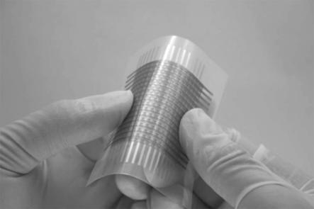
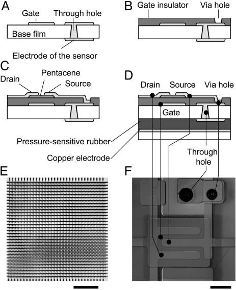
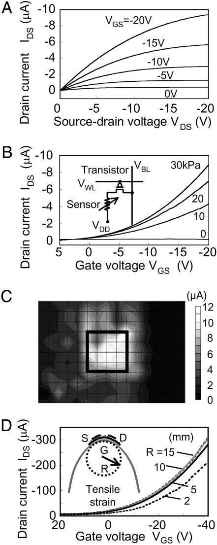
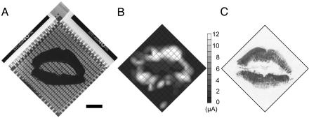
It is now widely accepted that skin sensitivity will be very important for future robots used by humans in daily life for housekeeping and entertainment purposes. Despite this fact, relatively little progress has been made in the field of pressure recognition compared to the areas of sight and voice recognition, mainly because good artificial "electronic skin" with a large area and mechanical flexibility is not yet available. The fabrication of a sensitive skin consisting of thousands of pressure sensors would require a flexible switching matrix that cannot be realized with present silicon-based electronics. Organic field-effect transistors can substitute for such conventional electronics because organic circuits are inherently flexible and potentially ultralow in cost even for a large area. Thus, integration of organic transistors and rubber pressure sensors, both of which can be produced by low-cost processing technology such as large-area printing technology, will provide an ideal solution to realize a practical artificial skin, whose feasibility has been demonstrated in this paper. Pressure images have been taken by flexible active matrix drivers with organic transistors whose mobility reaches as high as 1.4 cm(2)/V.s. The device is electrically functional even when it is wrapped around a cylindrical bar with a 2-mm radius.


Figures

Fig. 1.
Fig. 1.
Image of an electronic artificial skin. Organic transistors are used to realize a flexible active matrix, which is used to read out pressure images from the sensors. The device is bendable because all of the layers with the exception of the electrodes are made of soft materials.
Fig. 2.
Fig. 2.
Manufacturing process flow. (A) Through holes are drilled through a poly(ethylene naphthalate) (PEN) base film by a CO2 laser drill machine. Then both sides of the base film are coated by 150-nm-thick gold with 5-nm-thick chromium adhesion layers in the vacuum evaporator with shadow masks. One side of the gold layer is also used as the gate electrodes of organic transistors. (B) A 500-nm-thick polyimide layer is prepared by spin coating as a gate dielectric layer. Then some areas of the polyimide layer are removed by the CO2 laser drill machine to make contact via holes. (C) A 50-nm-thick pentacene layer is deposited in the vacuum sublimation system. Then a 50-nm-thick gold layer is deposited through a shadow mask for the source and drain electrodes. (D) A pressure-sensitive rubber sheet and a copper electrode suspended by a polyimide film are laminated to the bottom of the PEN film with the transistors. (E) A picture of a 32 × 32 array of sensor cells (SENCELs). The pitch is 2.54 mm. (Scale bar = 2 cm.) (F) A magnified image of a SENCEL (2.54 × 2.54 mm2). (Scale bar = 0.5 mm.)
Fig. 3.
Fig. 3.
Device characteristics. (A) Drain current (IDS) measured for the transistors with pentacene as a channel layer, showing p-type conduction. The source–drain voltage (VDS) is swept from 0 V to -20 V under gate bias (VGS) from 0 V to -20 V with -5-V steps. (B) Transfer curves (IDS vs. VGS) are measured for a SENCEL under application of various pressures from 0 to 30 kPa. VDS = -20 V is applied. The resistance of the pressure-sensitive conductive rubber changes between 10 MΩ and 1 kΩ when it is off and on. (Inset) The circuit diagram of each SENCEL is shown. VBL, bit line; VWL, word line; VDD, supply voltage. (C) The fabricated sensor matrix is pressed with a rectangular rubber block. The position dependence of the drain current is monitored with applying voltage bias of VDS =-20 V and VGS =-20 V. The solid square indicates where the rubber block was positioned. (D) The transfer curves (IDS vs. VGS) are measured for a pentacene transistor rolled around cylindrical bars with various radii as schematically shown in the Inset. S, source; D, drain; G, gate. The channel length (L) and width (W) are 50 μm and 16 mm, respectively. The electronic performance does not change when the bending radius (R) is changed from 50 to 10 mm. Further reduction of R causes decrease of drain current IDS, but the transistor is still functional even at R = 2 mm.
Fig. 4.
Fig. 4.
A pressure image of a kiss mark is taken by using the present sensors. The device, consisting of 16 × 16 SENCELs, is pressed with a lip-shaped rubber replica (A) and the pressure image (B) is compared with the print on paper (C). The current of each SENCEL is measured with a -20-V operating bias. The two bright spots at the bottom of B are due not to a failure of transistors but to a failure of sensors around those two spots (low local resistance of the pressure-sensitive rubber). (Scale bar = 1 cm.)

Similar articles

Cited by

References

    1. Nicholls, H. R. & Lee, M. H. (1989) Int. J. Robotics Res. 8, 3-30.
    1. Lee, M. H. & Nicholls, H. R. (1999) Mechatronics 9, 1-31.
    1. Tsumura, A., Koezuka, H. & Ando, T. (1986) Appl. Phys. Lett. 49, 1210-1212.
    1. Burroughes, J. H., Jones, C. A. & Friend, R. H. (1988) Nature 335, 137-141.
    1. Sirringhaus, H., Tessler, N. & Friend, R. H. (1998) Science 280, 1741-1744. - PubMed

Publication types

LinkOut - more resources