

doi: 10.1073/pnas.0502848102.
Epub 2005 Jul 18.
Two-dimensional atomic crystals
Affiliations
- PMID: 16027370
- PMCID: PMC1180777
- DOI: 10.1073/pnas.0502848102
Item in Clipboard
Two-dimensional atomic crystals
Proc Natl Acad Sci U S A.
.
Abstract
We report free-standing atomic crystals that are strictly 2D and can be viewed as individual atomic planes pulled out of bulk crystals or as unrolled single-wall nanotubes. By using micromechanical cleavage, we have prepared and studied a variety of 2D crystals including single layers of boron nitride, graphite, several dichalcogenides, and complex oxides. These atomically thin sheets (essentially gigantic 2D molecules unprotected from the immediate environment) are stable under ambient conditions, exhibit high crystal quality, and are continuous on a macroscopic scale.
Figures
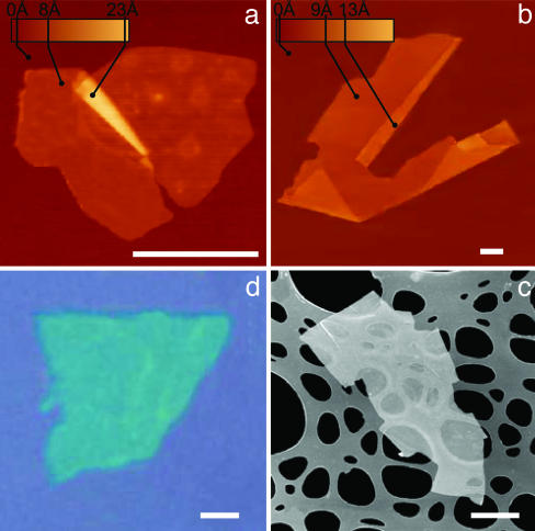
2D crystal matter. Single-layer crystallites of NbSe2 (a), graphite (b), Bi2Sr2CaCu2Ox (c), and MoS2 (d) visualized by AFM (a and b), by scanning electron microscopy (c), and in an optical microscope (d). (All scale bars: 1 μm.) The 2D crystallites are on top of an oxidized Si wafer (300 nm of thermal SiO2) (a, b, and d) and on top of a holey carbon film (c). Note that 2D crystallites were often raised by an extra few angstroms above the supporting surface, probably because of a layer of absorbed water. In such cases, the pleated and folded regions seen on many AFM images and having the differential height matching the interlayer distance in the corresponding 3D crystals help to distinguish between double-layer crystals and true single sheets such as those shown here.
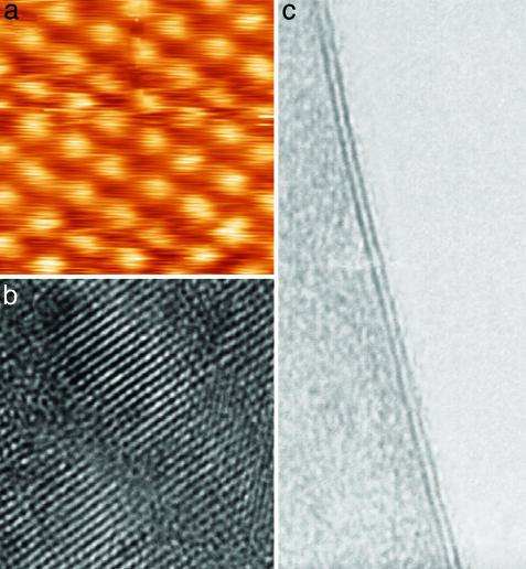
Atomic-resolution images of 2D materials. (a) Unfiltered scanning tunneling microscopy image of the crystal lattice in the NbSe2 monolayer on top of an oxidized Si wafer. Note that for the scanning tunneling microscopy measurements, an Au film was deposited around 2D crystallites to provide an electrical contact. (b) HRTEM images of the 2D Bi2Sr2CaCu2Ox crystal shown in Fig. 1c. (c) HRTEM image of a double-layer MoS2. This image is shown to make a connection between our approach based on AFM identification of 2D crystals and the traditional HRTEM approach used for quasi-1D crystals (all nanotubes were first found by using HRTEM, where dark lines indicating the nanotube's walls parallel to the electron beam are easily visible). No similar signature exists for 2D crystals (see refs. 6-8), and we also found it difficult to align 2D samples exactly parallel to the electron beam. However, for two-layer crystals, their thickness is easily identifiable not only in AFM but also in HRTEM because of folded regions seen as two dark lines (in the case of c, the separation is ≈6.5 Å, in agreement with the interlayer distance in bulk MoS2). We occasionally observed short dark lines (compare with ref. 8) that might be folded monolayers, but no independent proof for this (e.g., by simultaneous AFM studies) has been obtained yet.
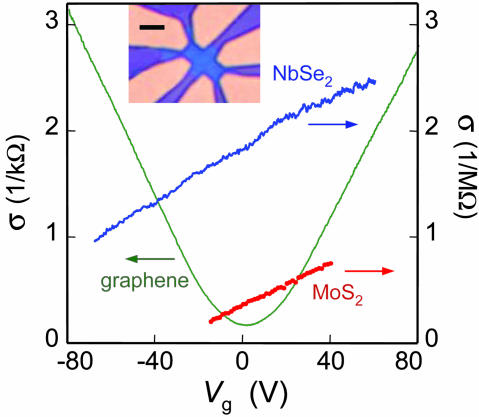
Electric field effect in single-atomic-sheet crystals. Changes in electrical conductivity σ of 2D NbSe2, 2D MoS2, and graphene as a function of gate voltage are shown (300 K). (Inset) Our typical devices used for such measurements: It is an optical image (in white light) of 2D NbSe2 on top of an oxidized Si wafer (used as a gate electrode) with a set of Au contacts. The crystal is seen as a bluer region in the center. (Scale bar: 5 μm.)
References
-
- Kroto, H. W., Fischer, J. E. & Cox, D. E., eds. (1993) The Fullerenes (Pergamon, Oxford).
-
- Iijima, S. (1991) Nature 354, 56-58.
-
- Chopra, N. G., Luyken, R. J., Cherrey, K., Crespi, V. H., Cohen, M. L., Louie, S. G. & Zettl, A. (1995) Science 269, 966-967. - PubMed
-
- Tenne, R., Margulis, L., Genut, M. & Hodes, G. (1992) Nature 360, 444-446.
-
- Dresselhaus, M. S. & Dresselhaus, G. (2002) Adv. Phys. 51, 1-186.
LinkOut - more resources
Full Text Sources
Other Literature Sources
