. 2005 Aug;52(8):1470-7.
doi: 10.1109/TBME.2005.851478.

An array of microactuated microelectrodes for monitoring single-neuronal activity in rodents

Affiliations

An array of microactuated microelectrodes for monitoring single-neuronal activity in rodents

Jit Muthuswamy et al. IEEE Trans Biomed Eng. 2005 Aug.

Abstract

Arrays of microelectrodes used for monitoring single- and multi-neuronal action potentials often fail to record from the same population of neurons over a period of time for several technical and biological reasons. We report here a novel Neural Probe chip with a 3-channel microactuated microelectrode array that will enable precise repositioning of the individual microelectrodes within the brain tissue after implantation. Thermal microactuators and associated microelectrodes in the Neural Probe chip are microfabricated using the Sandia's Ultraplanar Multi-level MEMS Technology (SUMMiTV) process, a 5-layer polysilicon micromachining technology of the Sandia National labs, Albuquerque, NM. The Neural Probe chip enables precise bi-directional positioning of the microelectrodes in the brain with a step resolution in the order of 8.8 microm. The thermal microactuators allow for a linear translation of the microelectrodes of up to 5 mm in either direction making it suitable for positioning microelectrodes in deep structures of a rodent brain. The overall translation in either direction was reduced to approximately 2 mm after insulation of the microelectrodes with epoxy for monitoring multi-unit activity. Single unit recordings were obtained from the somatosensory cortex of adult rats over a period of three days demonstrating the feasibility of this technology. Further optimization of the microelectrode insulation and chip packaging will be necessary before this technology can be validated in chronic experiments.


Figures

None
Jit Muthuswamy received the B. Tech. degree in electrical and electronic communication engineering from the Indian Institute of Technology, Kharagpur, India, in 1991. He received the M.S. and Ph.D. degrees in biomedical engineering in 1993 and 1996, respectively, and the MS degree in electrical engineering in 1996, all from Rensselaer Polytechnic Institute, Troy, NY. He is currently an Assistant Professor with the Harrington Department of Bioengineering at Arizona State University, Tempe. His research interests are in BioMEMS and brain injury.
None
Murat Okandan received the B.S., M.S., and Ph.D. degrees in electrical engineering from the Pennsylvania State University, Philadelphia, in 1994, 1995 and 1998, respectively. Since 1999, he has been with Sandia National Laboratories, Albuquerque, NM, where he is involved in microsystems technology and project development. His research interests include ultrathin gate dielectrics, enhanced micromachining technologies, and novel device concepts with applications in biological, medical, and sensing systems.
None
Aaron Gilletti received the B.S. and M.S. degree from the Harrington Department of Bioengineering at the Arizona State University, Tempe, in 2001 and 2003, respectively. His research interests include BioMEMS technologies for neural interfaces and his thesis work involved BioMEMS for neuro-electrophysiology signal acquisition and the quantification of tissue micromotion.
None
Michael S. Baker received the M.S. degree in mechanical engineering from Brigham Young University, Provo, UT, in 2002. He is currently a Senior Member of the Technical Staff in the MEMS Device Concepts department at Sandia National Laboratories, Albuquerque, NM. His research efforts are in the area of MEMS bistable mechanisms, compliant mechanism design, and actuation.
None
Tilak Jain received the B.Tech. degree in instrumentation engineering from the Indian Institute of Technology (IIT), Kharagpur, India, in 2002. He is currently a doctoral student in the Harrington Department of Bioengineering at Arizona State University, Tempe. His research interests include BioMEMS technologies for neural interfaces, genetic engineering, and other biotechnological applications.
Fig. 1
Fig. 1
Principle of thermal actuation—slightly angled pair of polysilicon strips on either side of a polysilicon shuttle in the center expand in plane upon heating and move the shuttle down. In our design, two such thermal actuators were used to achieve up and down motion of the shuttle, respectively. In addition, four more thermal actuators (two on either side of the shuttle) were used to engage and disengage locks during motion in either direction. The locks remain engaged in the inactive state and were disengaged only when the actuators controlling the locks were activated. Two actuators were dedicated to release the up-lock and two to release the down-lock upon activation.
Fig. 2
Fig. 2
Computer-aided design layout of one of the polysilicon microelectrode (shown in dark grey running down the middle of the layout) and associated thermal microactuators. The contact pads are shown in light grey.
Fig. 3
Fig. 3
Micrographs of (a) complete drive mechanism and (b) zoomed view of the top half of the actuator. The 5 bond pads (move up, move down, actuator-up lock, actuator-down lock and ground pads) that are used to energize the microactuator are visible in (a). The counter-translation latch and ratchet pawl are engaged in a lock position in (b).
Fig. 4
Fig. 4
Micrograph showing two thermal actuators energized to pull and release the counter-translation latches and ratchet pawls on either side of the microelectrode (shuttle) to disengage them and allow translation of the microelectrode in the downward direction.
Fig. 5
Fig. 5
Schematic of the SUMMiTV process indicating the different layers of polysilicon available for fabricating mechanical and electrical components.
Fig. 6
Fig. 6
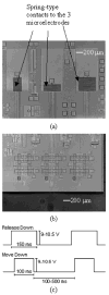
(a). Spring-type leads make electrical contact from stationary bond pads to the top of the moving microelectrodes. The springs-type leads are either 1.6 mm or 3.2 mm long and have no spring constant to mechanically retract the microelectrode. They just make electrical contact with a resistance of approximately 10 kΩ. (b). A close-up of the bottom edge of the 3-channel neural probe chip showing the three adjacent microactuators and associated microelectrodes poised to extend out of the chip. The microelectrodes are separated by approximately 800 μm. (c). Typical waveforms used to drive the thermal actuator probe. Voltage level is specific to each chip and the pulse duration and latency is dependent on the desired speed for driving the device.
Fig. 7
Fig. 7
A photograph of the 3-channel neural probe chip showing the end with two of the microelectrodes extended over the edge of the chip and the third microelectrode in the retracted position within the chip. The microelectrodes are epoxy insulated and separated by approximately 800 μm to minimize cross-channel electrical coupling. The chip is mounted on a standard DIP socket covered by glass slide to protect the microactuators and also to allow for visualization after implantation. The whole packaging weighs approximately 8.14 g and is suitable for chronic implantation on a rat head.
Fig. 8
Fig. 8
Impedance [magnitude in (a) and phase in (b)] spectra of epoxy-coated polysilicon microelectrodes dipped in phosphate buffered saline over a period of 6 days indicate stability in the impedance magnitude of the polysilicon-epoxy interface.
Fig. 9
Fig. 9
Multi-unit activity using the thermal microactuators over a period of 3 days (a) from channel 1 on day 2 and (b) from channel 2 on day 2. Multi-unit data after actuation by approximately 90 μm is also shown in (b). Data from (c) channel 1 on day 3 shows subdued neuronal activity with only one single unit in the inset and (d) channel 2 on day 3. The insets display multiple occurrences of single unit activity after sorting.

References

    1. BeMent SL, Wise KD, Anderson D, Najafi K, Drake KL. Solid state electrodes for multi channel multi-plexed intracortical neuronal recording. IEEE Trans Biomed Eng. 1986;BME-33:230–240. - PubMed
    1. Charles HK, Massey JT, Mountcastle VB. Polyimides as insulating layers for implantable electrodes. In: Mittal KL, editor. Polyimides. Vol. 2. New York: Plenum; 1984. pp. 1139–1155.
    1. Eichenbaum H, Kuperstein M. Extracellular neural recording with multichannel microelectrodes. J Electrophysiol Tech. 1986;13:189–209.
    1. Kuperstein M, Whittington DA. A practical 24 channel microelectrode for neural recording in vivo. IEEE Trans Biomed Eng. 1981;BME-28:288–293. - PubMed
    1. Pickard RS. A review of printed circuit microelectrodes and their production. J Neurosci Methods. 1979;1:301–319. - PubMed

Publication types