. 2006 Feb 28;34(4):e32.
doi: 10.1093/nar/gnj034.

Controlled loading of oligodeoxyribonucleotide monolayers onto unoxidized crystalline silicon; fluorescence-based determination of the surface coverage and of the hybridization efficiency; parallel imaging of the process by Atomic Force Microscopy

Affiliations

Controlled loading of oligodeoxyribonucleotide monolayers onto unoxidized crystalline silicon; fluorescence-based determination of the surface coverage and of the hybridization efficiency; parallel imaging of the process by Atomic Force Microscopy

Fabrizio Cattaruzza et al. Nucleic Acids Res. .

Abstract

Unoxidized crystalline silicon, characterized by high purity, high homogeneity, sturdiness and an atomically flat surface, offers many advantages for the construction of electronic miniaturized biosensor arrays upon attachment of biomolecules (DNA, proteins or small organic compounds). This allows to study the incidence of molecular interactions through the simultaneous analysis, within a single experiment, of a number of samples containing small quantities of potential targets, in the presence of thousands of variables. A simple, accurate and robust methodology was established and is here presented, for the assembling of DNA sensors on the unoxidized, crystalline Si(100) surface, by loading controlled amounts of a monolayer DNA-probe through a two-step procedure. At first a monolayer of a spacer molecule, such as 10-undecynoic acid, was deposited, under optimized conditions, via controlled cathodic electrografting, then a synthetic DNA-probe was anchored to it, through amidation in aqueous solution. The surface coverage of several DNA-probes and the control of their efficiency in recognizing a complementary target-DNA upon hybridization were evaluated by fluorescence measurements. The whole process was also monitored in parallel by Atomic Force Microscopy (AFM).


Figures

Scheme 1
Scheme 1
Overall procedure.
Figure 1
Figure 1
Dependence of the maximum intensity emission (λem = 520 nm, λex = 492 nm) of ODN 2 Fluorescein-5′-dT20-3′-Hexyl-NH2 on its concentration in Tris–HCl buffer after digestion with Phosphodiesterase I (straight line, closed circle) and of 1 ODN Fluorescein-5′-dA20-3′ in urea 7 M (dashed line, closed inverted triangle).
Figure 2
Figure 2
Solution fluorescence intensity versus time, during the enzymatic digestion of an amino-terminated oligonucleotide (2) immobilized on the silicon surface.
Figure 3
Figure 3
AFM contact mode topographic images (5 × 5 µm) of 10-undecynoic acid CEG deposited on Si(100) surface at high cathodic charge density (1200 mC/cm2), showing non-homogeneity and aggregation (A). The white bar indicates the analysed zone. The cross section profile (B) is measured along the bar.
Figure 4
Figure 4
(A) AFM contact mode and (B) friction force topographic images (2 × 2 µm) of 10-undecynoic acid CEG deposited on Si(100) surface with at 12 mC/cm2 cathodic charge density. The surface appears less homogeneous than as in well-covered monolayers. Round, so called ‘friction holes’ appear in the friction image, matching the higher areas in the contact mode topographic image. The white bar indicates the analysed zone. The corresponding cross section profiles, measured along the bar, are reported below, in (C and D), respectively.
Figure 5
Figure 5
AFM tapping mode topographic image (A) (6 × 6 µm) of 10-undecynoic acid CEG deposited on Si(100) surface at 36 mC/cm2 cathodic charge density and covered with a very low concentration of ssODN 2. The non-functionalized area allows to define as ca. 1.5 nm the height of the 10-undecynoic acid layer on the surface. The ODN molecules are represented as small round structures. The white bar indicates the analysed zone. The cross section profile (B) is measured along the bar. It should be noted that the scratch profile line is fairly smooth, and the local corrugation of the monolayer is consistent with the uniform monolayer.
Scheme 2
Scheme 2
Amidation reaction mechanism.
Figure 6
Figure 6
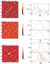
Panel 1: AFM tapping mode topographic image (1 × 1 µm) of a Si(100) surface covered with a uniform layer of 10-undecynoic acid using a CEG procedure at 120 mC/cm2 cathodic charge density. The white bar indicates the analysed zone. The cross section evidences that the mean corrugation of the sample is around 1.3 nm. Panel 2: AFM tapping mode topographic image (1 × 1 µm) of a sample covered with 20mer ODN 1 (nominal density 5.63 × 10¹² strands/cm2). The cross sections A and B show structures ca. 18 nm wide and ca. 3 nm high. The white bar indicates the analysed zone. The vertical heights, as measured along the bars, are reported in A and B. Panel 3: AFM tapping mode topographic image (1 × 1 µm) of a sample covered with a dsODN 1 + 4 (nominal density 5.63 × 10¹² strands/cm2). The molecules appear as rod-like structures. Cross section A shows a structure ca. 20 nm wide and ca. 1.5 nm high. The height is lower than that of ssODN 1 (ca. 3 nm), probably due to a different orientation of the molecules on the surface. Cross section B, taken on a large agglomerate, can be deconstructed in three smaller structures with dimensions, shown by the fit curves, comparable with the dimensions of single molecules. The formation of large structures appears to be a side-effect of the hybridization process, as reported in the literature for similar samples (41). The white bar indicates the analysed zones. The cross section profiles as measured along the bar, without and with deconvolution of the profile, are reported in A and B, respectively.
Figure 7
Figure 7
Panel 1: AFM tapping mode topographic image (A), (250 × 250 nm) of a sample covered with a low concentration (nominal density ca. 1011 strands/cm2) of 20mer ODN 1, acquired by the use of super-tips (apical radius ca. 2 nm). The cross section shows a structure ca. 8 nm wide and ca. 1.8 nm high. The different lateral dimensions of these structures compared with the samples analysed with the standard tips (apical radius ca. 30 nm) illustrates the importance of the apical radius and form. The different vertical dimensions are probably the effect of the greater tip pressure due to the much smaller contact area. The white bar indicates the analysed zone. The cross section profile, as measured along the bar, is reported in (B). Panel 2: AFM tapping mode topographic image (A), (1 × 1 µm) of a sample covered with a very low concentration (nominal density around 1010 strands/cm2) of 20mer ODN 1. The low concentration allows to unequivocally analyse every single molecule. The white bar indicates the analysed zone. The cross section (B) shows that the structures are ca. 25 nm wide and ca. 2.5 nm high.

Similar articles

Cited by

References

    1. Ball P. Silicon still supreme. Nature Mater. 2005;4:119. - PubMed
    1. Hersam M.C., Guisinger N.P., Lydin J.W. Silicon-based molecular nanotechnology. Nanotechnology. 2000;11:70–76.
    1. Yin H.B., Brown T., Greef R., Wilkinson J.S., J.Melvin J. Chemical modification and micropatterning of Si(100) with oligonucleotides. Microelectronic Eng. 2004;73–74:830–836.
    1. Herne T.M., Tarlov M.J. Characterization of DNA probes immobilized on gold surfaces. J. Am. Chem. Soc. 1997;119:8916–8920.
    1. Peterlinz K.A., R.M.Georgiadis R.M. Observation of hybridisation and dehybridisation of thiol-tethered DNA using two-color surface plasmon resonance spectroscopy. J. Am. Chem. Soc. 1997;119:3401–3402.

Publication types

MeSH terms