

doi: 10.1021/nl060994c.
Two-dimensional nanoparticle arrays show the organizational power of robust DNA motifs
Affiliations
- PMID: 16834438
- PMCID: PMC3465979
- DOI: 10.1021/nl060994c
Item in Clipboard
Two-dimensional nanoparticle arrays show the organizational power of robust DNA motifs
Nano Lett.
2006 Jul.
Abstract
The bottom-up spatial organization of potential nanoelectronic components is a key intermediate step in the development of molecular electronics. We describe robust three-space-spanning DNA motifs that are used to organize nanoparticles in two dimensions. One strand of the motif ends in a gold nanoparticle; only one DNA strand is attached to the particle. By using two of the directions of the motif to produce a two-dimensional crystalline array, one direction is free to bind gold nanoparticles. Identical motifs, tailed in different sticky ends, enable the two-dimensional periodic ordering of 5 and 10 nm diameter gold nanoparticles.
Figures
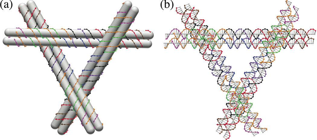
(a) A Schematic of the Motif. In this schematic diagram, double helices are shown as opaque rods around which the individual strands are wrapped. Note the 3-space-spanning character of the three DX domains. (b) A Detailed Molecular Structure. Each nucleotide is shown in a representation that illustrates a color-coded backbone virtual atom connected to its neighbors along the helix. A gray line representing the base is drawn from this atom to the helix axis, which is also drawn. Both diagrams drawn by the program Gideon..
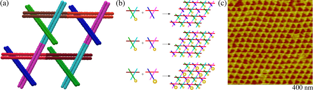
(a) A Schematic Showing the Formation of a Two-Component Array. Four triangles of two species in which each domain has been color coded are shown connected. The view parallel to the three-fold axes shows how only two domains (cyan bonding to magenta and brown bonding to red) are involved in array formation, while the end of the third domain (blue or green) is free to be involved in scaffolding operations. (b) Diagrams Showing the Attachment of Nanoparticles. The color-coding is the same as in (a). This view is perpendicular to the rhombic surfaces of the 2D array. Its three panels show, top to bottom, 5 nm particles attached to only one of the two triangular tiles, 5 nm particles attached to both of the tiles, and 5 nm particles attached to one of the tiles and 10 nm particles attached to the other tile. (c) A Tapping-Mode Atomic Force Micrograph of an Underivatized Array. Note that despite a pseudo-trigonal appearance, the features in the lighter portion of the array are all parallel to each other, and there is no threefold axis at the centers of the triangles, nor at their vertices. There is a prominent high feature in the lower-left-to-upper-right direction that we interpret as the domain not involved in lattice formation.
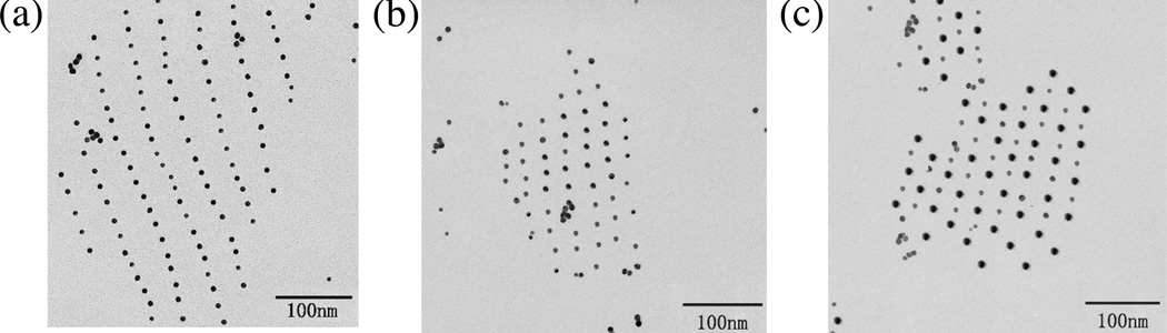
(a) An array where one tile contains 5 nm particles. It is clear that this arrangement results in one short distance and one long distance. Sometimes a particle is missing. (b) An array where both tiles contain 5 nm particles. The distances between particles are seen to be equal here. (c) An array where one tile contains a 5 nm particle and the other tile contains a 10 nm particle. The alternation of 5 nm particles and 10 nm particles is evident from this image. Note that the spacings are precise in both directions, and that the pattern mimics the rhombic pattern of the tile array.
Similar articles
-
Periodic square-like gold nanoparticle arrays templated by self-assembled 2D DNA Nanogrids on a surface.Nano Lett. 2006 Feb;6(2):248-51. doi: 10.1021/nl052210l. Nano Lett. 2006. PMID: 16464044
-
Switching binary states of nanoparticle superlattices and dimer clusters by DNA strands.Nat Nanotechnol. 2010 Feb;5(2):116-20. doi: 10.1038/nnano.2009.378. Epub 2009 Dec 20. Nat Nanotechnol. 2010. PMID: 20023646
-
Covalent Linkage of One-Dimensional DNA Arrays Bonded by Paranemic Cohesion.ACS Nano. 2015 Oct 27;9(10):10304-12. doi: 10.1021/acsnano.5b04335. Epub 2015 Sep 11. ACS Nano. 2015. PMID: 26343906
-
At the crossroads of chemistry, biology, and materials: structural DNA nanotechnology.Chem Biol. 2003 Dec;10(12):1151-9. doi: 10.1016/j.chembiol.2003.12.002. Chem Biol. 2003. PMID: 14700623 Review.
-
Patterning metallic nanoparticles by DNA scaffolds.Adv Exp Med Biol. 2007;620:107-16. doi: 10.1007/978-0-387-76713-0_8. Adv Exp Med Biol. 2007. PMID: 18217338 Review.
Cited by
-
DNA-linked superlattices get into shape.Nat Mater. 2015 Aug;14(8):746-9. doi: 10.1038/nmat4376. Nat Mater. 2015. PMID: 26201879 No abstract available.
-
Combing and self-assembly phenomena in dry films of Taxol-stabilized microtubules.Nanoscale Res Lett. 2007 Mar 13;2(3):135-43. doi: 10.1007/s11671-007-9044-x. Nanoscale Res Lett. 2007. PMID: 21806849 Free PMC article.
-
Self-assembly of biomolecular soft matter.Faraday Discuss. 2013;166:9-30. doi: 10.1039/c3fd00120b. Faraday Discuss. 2013. PMID: 24611266 Free PMC article.
-
Designer DNA nanoarchitectures.Biochemistry. 2009 Mar 3;48(8):1663-74. doi: 10.1021/bi802324w. Biochemistry. 2009. PMID: 19199428 Free PMC article. Review.
-
Position Accuracy of Gold Nanoparticles on DNA Origami Structures Studied with Small-Angle X-ray Scattering.Nano Lett. 2018 Apr 11;18(4):2609-2615. doi: 10.1021/acs.nanolett.8b00412. Epub 2018 Mar 6. Nano Lett. 2018. PMID: 29498287 Free PMC article.
References
-
- Alivisatos AP. J. Phys. Chem. 1996;100:13226–13239.
- Redl FX, Cho KS, Murray CB, O'Brien S. Nature. 2003;423:978–971. - PubMed
-
- Kiehl RA. J. Nanopart. Res. 2000;2:331–332.
-
- Likharev KK. Electronics Below 10 nm. In: Greer J, Korkin A, Labanowski J, editors. Nano and Giga Challenges in Microelectronics. Amsterdam: Elsevier; 2003. pp. 27–68.
- Maier SA, Brongersma ML, Kik PG, Meltzer S, Requicha AAG, Atwater HA. Adv. Mater. 2001;13:1501–1505.
- Shipway AN, Katz E, Willner I. ChemPhysChem. 2000;1:18–52. - PubMed
-
- Alivisatos A, Johnsson K, Peng X, Wilson T, Lowth C, Bruchez M, Schultz P. Nature. 1996;382:609–611. - PubMed
- Loweth C, Caldwell W, Peng X, Alivisatos P, Schultz P. Angew. Chem. Int. Ed. 1999;38:1808–1812. - PubMed
- Zanchet D, Micheel C, Parak W, Alivisatos P. Nano Lett. 2001;1:32–35.
- Zanchet D, Micheel C, Parak W, Alivisatos P. J. Phys. Chem. B. 2002;106:11758–11763.
-
- Mucic R, Storhoff J, Letsinger R, Mirkin C. Nature. 1996;382:607–609. - PubMed
- Storhoff J, Elghenian R, Mucic R, Mirkin C. J. Am. Chem. Soc. 1998;120:1959–1964.
- Jin R, Wu G, Li Z, Mirkin C, Schatz G. J. Am. Chem. Soc. 2003;125:1643–1654. - PubMed
- Anderson CJ, Sykes TJ, Kornberg RD. Proc. Nat. Acad. Sci. (USA) 2005;102:13383–13385. - PMC - PubMed
Publication types
MeSH terms
Substances
Grants and funding
LinkOut - more resources
Full Text Sources
Other Literature Sources
