. 2006 Aug 1;103(31):11452-6.
doi: 10.1073/pnas.0601675103. Epub 2006 Jul 19.

Chemoresponsive monolayer transistors

Affiliations

Chemoresponsive monolayer transistors

Xuefeng Guo et al. Proc Natl Acad Sci U S A. .

Abstract

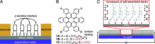
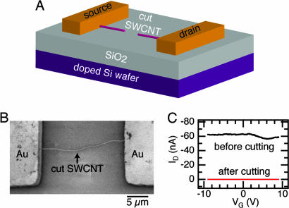
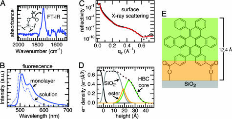
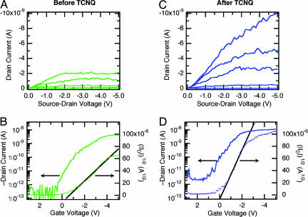
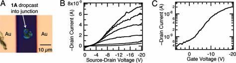
This work details a method to make efficacious field-effect transistors from monolayers of polycyclic aromatic hydrocarbons that are able to sense and respond to their chemical environment. The molecules used in this study are functionalized so that they assemble laterally into columns and attach themselves to the silicon oxide surface of a silicon wafer. To measure the electrical properties of these monolayers, we use ultrasmall point contacts that are separated by only a few nanometers as the source and drain electrodes. These contacts are formed through an oxidative cutting of an individual metallic single-walled carbon nanotube that is held between macroscopic metal leads. The molecules assemble in the gap and form transistors with large current modulation and high gate efficiency. Because these devices are formed from an individual stack of molecules, their electrical properties change significantly when exposed to electron-deficient molecules such as tetracyanoquinodimethane (TCNQ), forming the basis for new types of environmental and molecular sensors.


Conflict of interest statement

Conflict of interest statement: No conflicts declared.

Figures

Fig. 1.
Fig. 1.
A schematic of how HBCs can be formed into a monolayer and measured with ultrasmall point contacts. (A) An alternative molecular electronics where molecules are attached through the X-group to a primer layer for assembly and probed laterally. The semiconductor/air interface should be very sensitive to its environment. (B) HBC molecules. 1A assembles into 1D stacks. 1B and 1C synthesized with groups to bind them to the surface of silicon oxide. (C) Monolayers of self-assembled stacks being probed with SWNT electrodes separated by only a few nanometers.
Fig. 2.
Fig. 2.
The electrodes are formed by cutting an individual, metallic SWNT. (A) A cut SWNT on a doped silicon wafer contacted by large metal pads. The cut nanotube serves as the S/D electrodes, and the silicon wafer acts as the global back-gate for the device. (B) SEM micrograph of an individual SWNT between gold electrodes after being oxidatively cut. (C) Electrical properties (ID vs. VG at VD = −50 mV) of a metallic tube before (black trace) and after (red trace) oxidative cutting.
Fig. 3.
Fig. 3.
The HBCs form dense, upright monolayers on the surface of silicon oxide. (A) Carbonyl region of the FTIR spectrum of a silicon wafer after reaction with 1B. (B) Comparison of solution (6.4 × 10⁻⁶ M in THF) and monolayer fluorescence emission of 1B (excitation at 385 nm). (C) Surface x-ray scattering of 1B. Data, black triangles; fit to a three-layer model (red line). (D) Real-space model of the fit from C showing the deconvolution of the electron density into three layers: silicon oxide, ester, and HBC. (E) Model with three layers color-coded to the real-space model.
Fig. 4.
Fig. 4.
Same device measured in Fig. 2C after the assembly of a monolayer of 1C on the SiO2 surface of a silicon wafer with a SWNT electrodes. (A) Transistor output, VG = 0 to −5 V in 1-V steps. (B) Transfer characteristics for the device, VD = −2 V. (C) Transistor output, VG = 0 to −5 V in 1-V steps, for the same device measured in A after treatment with a TCNQ solution (1 × 10⁻³ M in CH2Cl2). (D) Transfer characteristics for the device, VSD = −2 V.
Fig. 5.
Fig. 5.
Without the surface attachment, the device characteristics are poor. (A) Optical micrograph of a solution of 1A drop cast into a gap formed from SWNT electrodes. (B) Transistor output for 1A drop cast into a SWNT gap. The gate voltage ranges from 0 to −20 V in 4-V steps. (C) Transfer characteristics for 1A drop cast into the SWNT gaps, VSD = −20 V.

References

    1. Kagan C. R., Afzali A., Martel R., Gignac L. M., Solomon P. M., Schrott A. G., Ek B. Nano Lett. 2003;3:119–124.
    1. Tulevski G. S., Miao Q., Fukuto M., Abram R., Ocko B., Pindak R., Steigerwald M. L., Kagan C. R., Nuckolls C. J. Am. Chem. Soc. 2004;126:15048–15050. - PubMed
    1. Dimitrakopoulos C. D., Malenfant P. R. L. Adv. Mater. 2002;14:99–117.
    1. Kagan C. R., Andry P. Thin-Film Transistors. New York: Dekker; 2003.
    1. Dodabalapur A., Torsi L., Katz H. E. Science. 1995;268:270–271. - PubMed

Publication types

Substances

LinkOut - more resources