

doi: 10.1073/pnas.0605033103.
Epub 2006 Jul 27.
Beyond the metal-insulator transition in polymer electrolyte gated polymer field-effect transistors
Affiliations
- PMID: 16873547
- PMCID: PMC1567663
- DOI: 10.1073/pnas.0605033103
Item in Clipboard
Beyond the metal-insulator transition in polymer electrolyte gated polymer field-effect transistors
Proc Natl Acad Sci U S A.
.
Abstract
We have studied the carrier transport in poly(2,5-bis(3-tetradecylthiophen-2-yl)thieno[3,2-b]thiophene) field-effect transistors (FETs) at very high field-induced carrier densities (10(15) cm(-2)) using a polymer electrolyte as gate and gate dielectric. At room temperature, we find high current densities, 2 x 10(6) A/cm(2), and high metallic conductivities, 10(4) S/cm, in the FET channel; at 4.2 K, the current density is sustained at 10(7) A/cm(2). Thus, metallic conductivity persists to low temperatures. The carrier mobility in these devices is approximately 3.5 cm(2).V(-1).s(-1) at 297 K, comparable with that found in fully crystalline organic devices.
Conflict of interest statement
Conflict of interest statement: No conflicts declared.
Figures
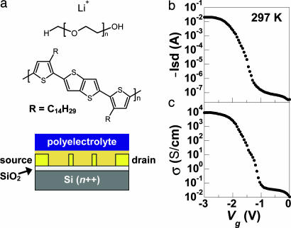
Polymer electrolyte gated FET structure and room temperature device characteristics. (a) A schematic illustration of the four-probe device structure complete with the ionic polymer electrolyte layer (Bottom) with the molecular structure shown (Top). The molecular structure of pBTTT-C14 is also shown (Middle). (b and c) Typical current vs. Vg (b) and conductivity vs. Vg (c) data measured for a device in ambient air at room temperature and Vsd = −1 V. The Vg sweep rate was ≈60 mV/s.
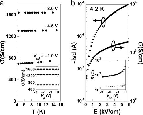
Low-temperature device characteristics. (a) Conductivity vs. temperature at varying Vsd for a device cooled beforehand from room temperature to 4.2 K while holding the gate bias constant at Vg = −3 V. (Inset) The conductivity vs. Vg at 4.2 K. (b) Current (and conductivity) vs. source–drain electric field for the same device shown in a, at 4.2 K. (Inset) The channel (filled circles) and contact (open circles) resistance vs. Vsd at 4.2 K.
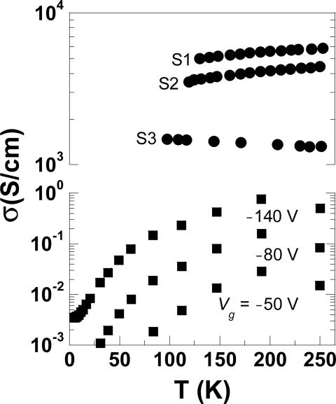
Conductivity vs. temperature for three polymer electrolyte gated (circles) devices at Vsd = −1 V. All devices were cooled beforehand to ≈260 K while holding the gate bias constant at Vg = −3 V. The data for a device without the electrolyte layer (squares), gated instead by using the bottom contact (SiO2, 200-nm thick), are shown at fixed Vsd = −60 V and varying Vg.
References
-
- Chiang C. K., Fincher C. R., Park Y. W., Heeger A. J., Shirakawa H., Louis E. J., Gau S. C., Macdiarmid A. G. Phys. Rev. Lett. 1977;39:1098–1101.
-
- Lee K., Cho S., Heum Park S., Heeger A. J., Lee C.-W., Lee S.-H. Nature. 2006;441:65–68. - PubMed
-
- Tal O., Rosenwaks Y., Preezant Y., Tessler N., Chan C. K., Kahn A. Phys. Rev. Lett. 2005;95:256405. - PubMed
-
- Dhoot A. S., Wang G. M., Moses D., Heeger A. J. , Phys. Rev. Lett. 2006;96:246403. - PubMed
-
- Bardeen J., Brattain W. H. Phys. Rev. 1948;74:230–231.
Publication types
MeSH terms
Substances
LinkOut - more resources
Full Text Sources
Other Literature Sources
Miscellaneous
