. 2006 Dec 20;128(50):16323-31.
doi: 10.1021/ja065923u.

Quantitative real-time measurements of DNA hybridization with alkylated nonoxidized silicon nanowires in electrolyte solution

Affiliations

Quantitative real-time measurements of DNA hybridization with alkylated nonoxidized silicon nanowires in electrolyte solution

Yuri L Bunimovich et al. J Am Chem Soc. .

Abstract

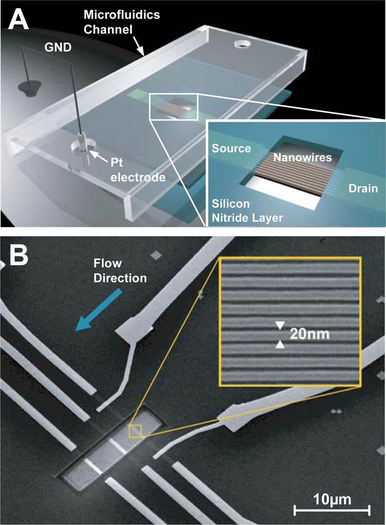
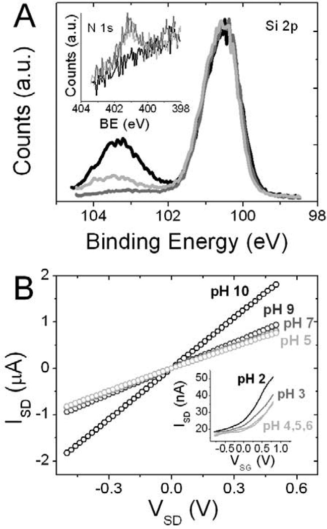
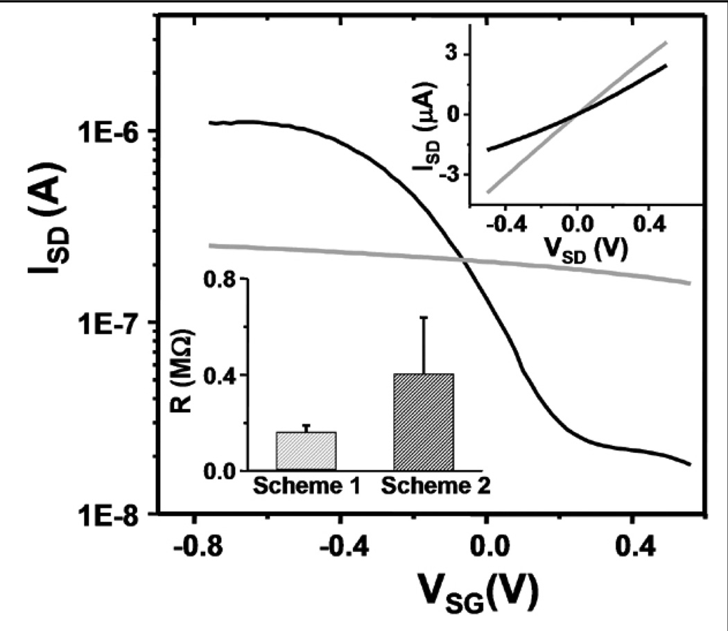
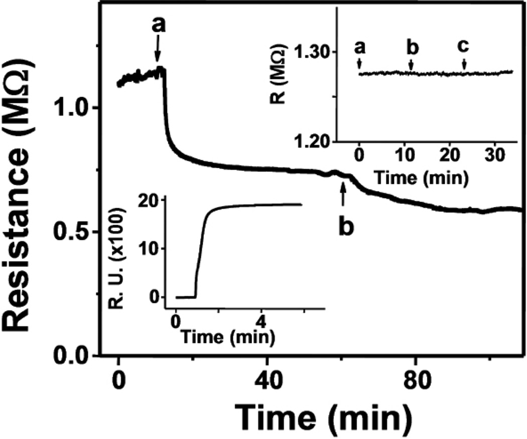
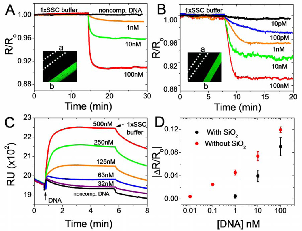
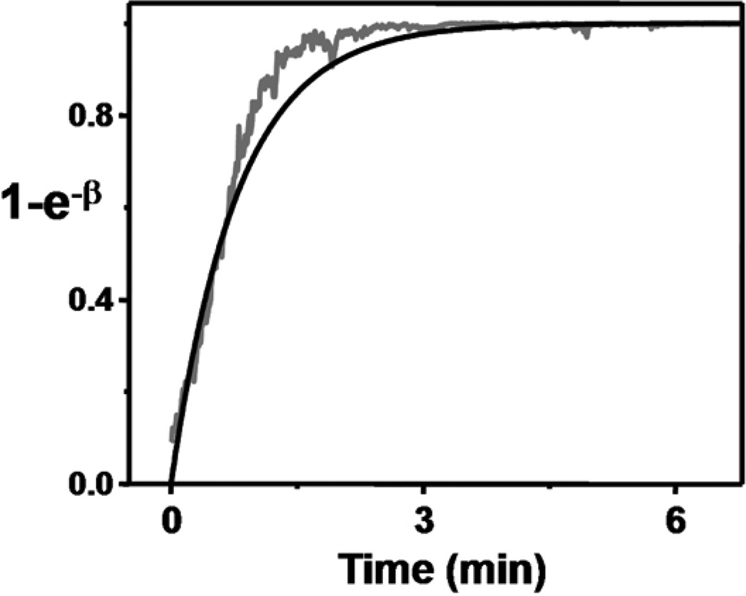
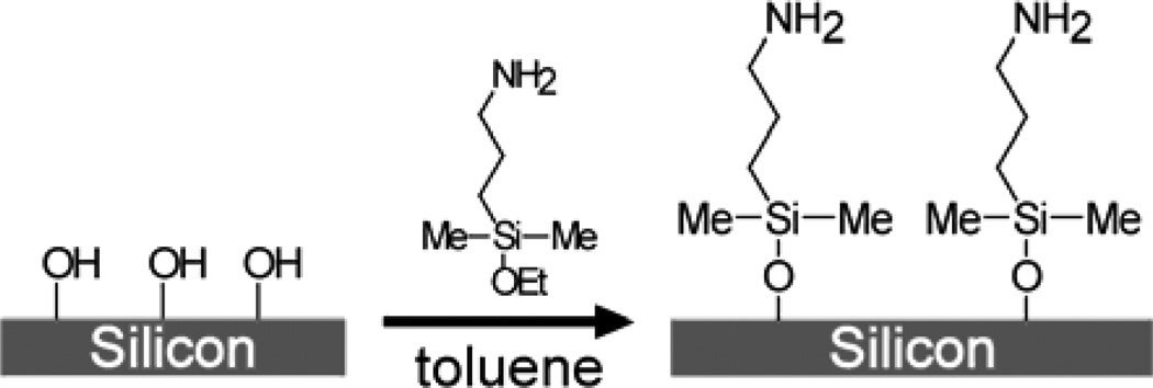
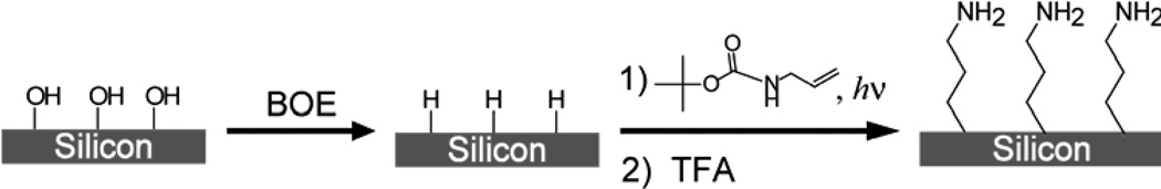
The quantitative, real-time detection of single-stranded oligonucleotides with silicon nanowires (SiNWs) in physiologically relevant electrolyte solution is demonstrated. Debye screening of the hybridization event is circumvented by utilizing electrostatically adsorbed primary DNA on an amine-terminated NW surface. Two surface functionalization chemistries are compared: an amine-terminated siloxane monolayer on the native SiO2 surface of the SiNW, and an amine-terminated alkyl monolayer grown directly on a hydrogen-terminated SiNW surface. The SiNWs without the native oxide exhibit improved solution-gated field-effect transistor characteristics and a significantly enhanced sensitivity to single-stranded DNA detection, with an accompanying 2 orders of magnitude improvement in the dynamic range of sensing. A model for the detection of analyte by SiNW sensors is developed and utilized to extract DNA-binding kinetic parameters. Those values are directly compared with values obtained by the standard method of surface plasmon resonance (SPR) and demonstrated to be similar. The nanowires, however, are characterized by higher detection sensitivity. The implication is that SiNWs can be utilized to quantitate the solution-phase concentration of biomolecules at low concentrations. This work also demonstrates the importance of surface chemistry for optimizing biomolecular sensing with silicon nanowires.


Figures

Figure 1
Figure 1
A diagram (A) and an SEM image (B) of a single device section containing three groups of ~10 SiNWs in a microfluidics channel. The wafer is covered with Si3N4 except for an exposed active region with SiNWs (A, inset; B). B, inset: High resolution SEM image of 20 nm SiNWs.
Figure 2
Figure 2
A. XPS of Si 2p region of Si(100) surface functionalized as in Scheme 2 before (dark grey) and after (light grey) TFA deprotection and 10 hrs in 1× SSC buffer. Nonfunctionalized Si(100) surface with native oxide (black). Inset: N 1s region of nonfunctionalized Si(100) surface (black), Si(100) functionalized by Scheme 1 (light grey) and Scheme 2 (dark grey). B. Current-Voltage (IV) graphs of SiNWs functionalized by Scheme 1 in solutions of varying pH. Inset: Solution gated (VSG) n-type hydroxyl terminated SiNW in solutions of varying pH.
Figure 3
Figure 3
Solution gating of SiNWs functionalized by Scheme 1 (grey) and by Scheme 2 (black) (VSD was 50 mV). (Right inset) IV curves of SiNWs in air with (black) and without (grey) oxide. (Left inset) Resistances in air of SiNWs functionalized by Scheme 1 (left) and Scheme 2 (right).
Figure 4
Figure 4
Real-time response of SiNWs functionalized as in Scheme 1 to the addition of (a) 10µM ssDNA and (b) 100nM complementary DNA. Right top inset: Real-time SiNW response to the sequential addition of (a) 0.165M SSC, (b) 0.0165M SSC, and (c) 0.00165M SSC buffers. Left inset: SPR measurement demonstrating the addition of 10µM ssDNA to poly-L-lysine coated CM5 sensor chip. VSD = 50mV.
Figure 5
Figure 5
Concentration-dependent, real-time sensing of complementary DNA by SiNWs and by SPR in 0.165M electrolyte. A. Real-time responses of SiNWs that were surface functionalized according to Scheme 1 and coated with electrostatically adsorbed primary DNA. The black trace represents exposure of the SiNW sensors to 100 nM non-complementary ssDNA. Each curve represents measurements from a different set of NWs. Inset: Fluorescence image of Si(100) surface (with overlaying PDMS microfluidics chip) treated as in Scheme 1 followed by 10µM primary DNA addition and addition of (microchannel a) 100nM noncomplementary fluorescent DNA and (microchannel b) 100nM complemenatary fluorescent DNA. PDMS chip was removed before the image was collected. B. As in A, except the SiNWs were functionalized according to Scheme 2. Inset: Same as in A inset, but Si(100) surface was treated as in Scheme 2. C. SPR measurement of the hybridization of complementary DNA to electrostatically adsorbed primary DNA on a poly-L-lysine surface. D. Normalized SiNW responses for Scheme 1 (black dots) and Scheme 2 (red dots) surface preparations, as a function of the log of DNA concentration. For all measurements, VSD = 50mV.
Figure 6
Figure 6
Comparison of SPR-derived hybridization kinetic parameters with NW sensing data. The black line represents eq. 5 plotted using kon and koff obtained from SPR measurements, β =(konC+koff)t. The grey trace is obtained from SiNW resistance versus time data, β=ΔRRmaxR. C=10 nM.
Scheme 1
Scheme 1
Functionalization of Si (100) Oxide Surface with Amine
Scheme 2
Scheme 2
Functionalization of Si (100) Surface with Amine

Similar articles

Cited by

References

    1. Kong J, Franklin NR, Zhou CW, Chapline MG, Peng S, Cho KJ, Dai H. Science. 2000;287:622. - PubMed
    1. Patolsky F, Lieber CM. Mater. Today. 2005;8:20.
    1. Park SJ, Taton TA, Mirkin CA. Science. 2002;295:1503. - PubMed
    1. Ziegler C. Analytical and Bioanalytical Chemistry. 2004;379:946. - PubMed
    1. Lasseter TL, Cai W, Hamers RJ. Analyst. 2004;129:3. - PubMed

Publication types