Review
. 2007 Jun 22;4(14):439-61.
doi: 10.1098/rsif.2006.0196.

Diamond and biology

Affiliations
Review

Diamond and biology

Christoph E Nebel et al. J R Soc Interface. .

Abstract

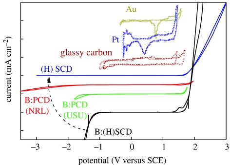
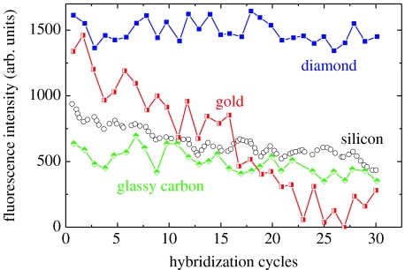
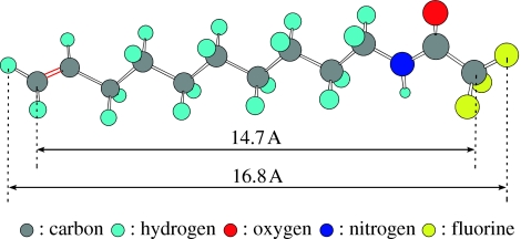
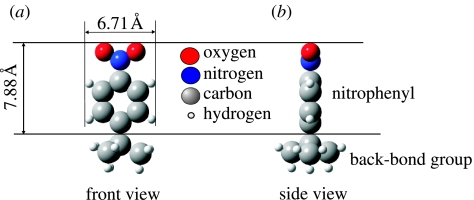
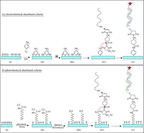
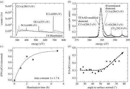
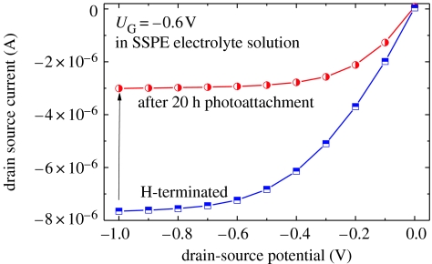
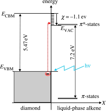
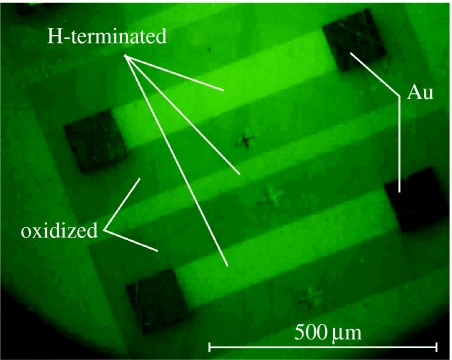
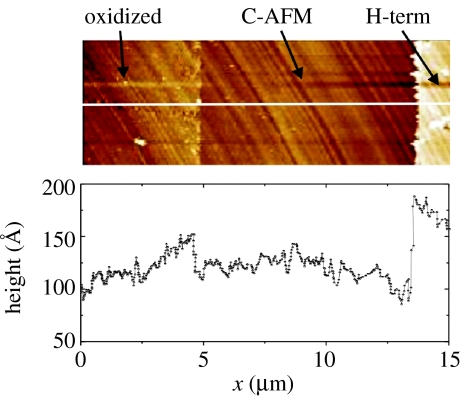
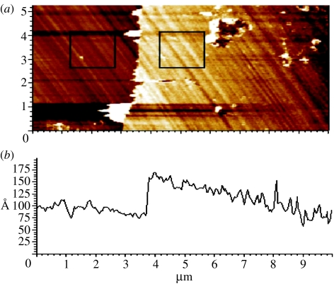
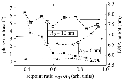
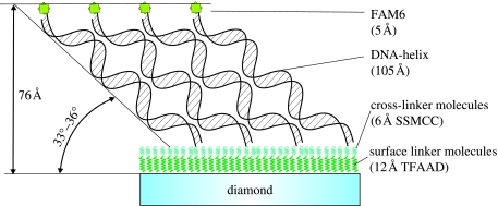
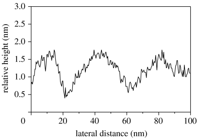
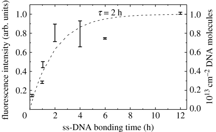
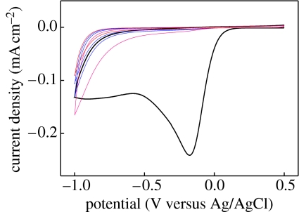
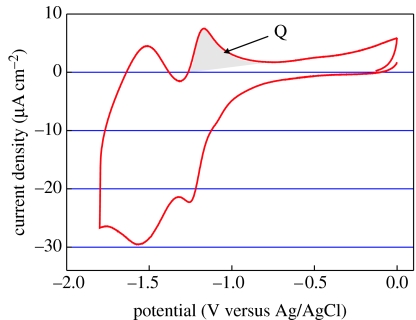
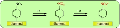
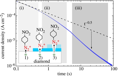
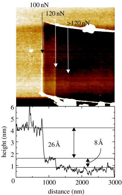
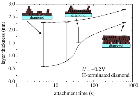
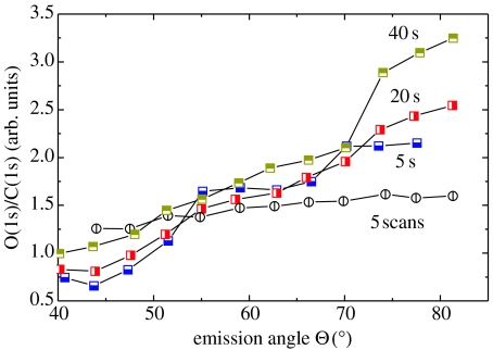
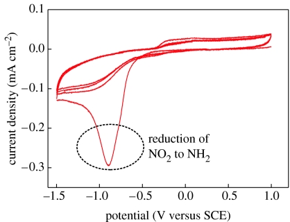
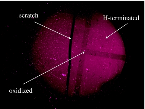
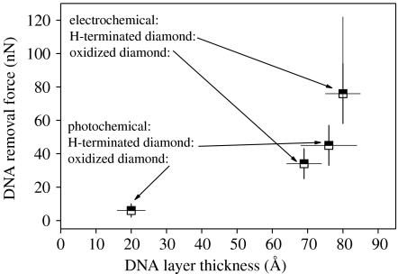
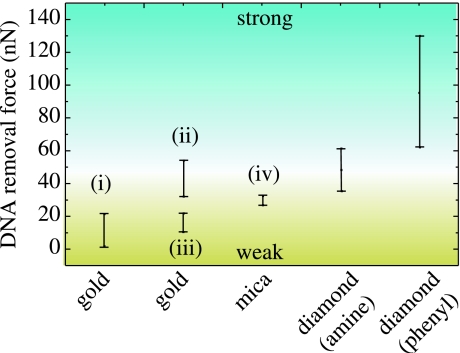
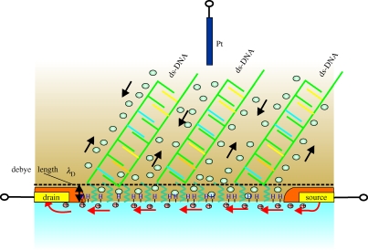
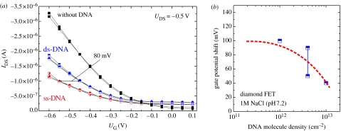
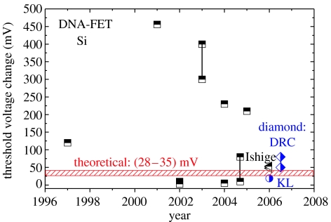
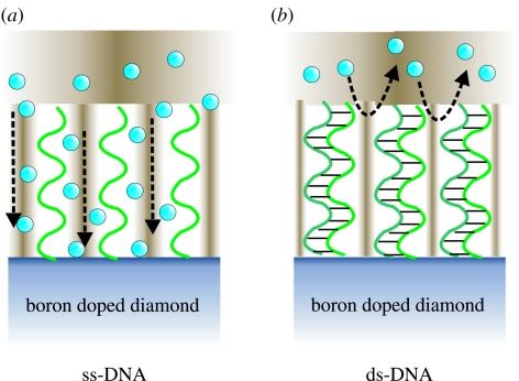
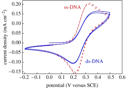
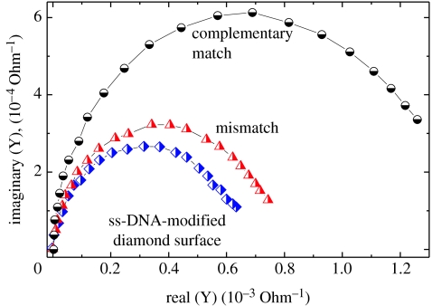
A summary of photo- and electrochemical surface modifications applied on single-crystalline chemical vapour deposition diamond films is given. The covalently bonded formation of amine and phenyl linker molecular layers is characterized using X-ray photoelectron spectroscopy, atomic force microscopy (AFM), cyclic voltammetry and field-effect transistor characterization experiments. Amine and phenyl layers are very different with respect to formation, growth, thickness and molecular arrangement. We deduce a sub-monolayer of amine linker molecules on diamond with approximately 10% coverage of 1.510(15) cm(-2) carbon bonds. Amine is bonded only on initially H-terminated surface areas. In the case of electrochemical deposition of phenyl layers, multilayer properties are detected with three-dimensional nitrophenyl growth properties. This leads to the formation of typically 25 A thick layers. The electrochemical bonding to boron-doped diamond works on H-terminated and oxidized surfaces. After reacting such films with heterobifunctional cross-linker molecules, thiol-modified ss-DNA markers are bonded to the organic system. Application of fluorescence and AFM on hybridized DNA films shows dense arrangements with densities up to 10(13) cm(-2). The DNA is tilted by an angle of approximately 35 degrees with respect to the diamond surface. Shortening the bonding time of thiol-modified ss-DNA to 10 min causes a decrease in DNA density to approximately 10(12) cm(-2). Application of AFM scratching experiments shows threshold removal forces of approximately 75 and 45 nN for the DNA bonded to the phenyl and the amine linker molecules, respectively. First, DNA sensor applications using Fe(CN6) 3-/4- mediator redox molecules and DNA field-effect transistor devices are introduced and discussed.


Figures

Figure 1
Figure 1
Voltammograms for water electrolysis of various electrodes. The supporting electrolyte is 0.5 M H2SO4. The graphs are shifted vertically for comparison. Two polycrystalline films, B : PCD(NRL) with 5×10¹⁹ B cm−3 and B : PCD(USU) with 5×10²⁰ B cm−3, from Granger et al. (2000) are compared with a single-crystalline boron-doped diamond B: (H)SCD with 3×10²⁰ B cm−3 and with an undoped diamond (H)SCD. Oxidation reactions, e.g. oxygen evolution, have positive currents and emerge around 1.8 V for all diamond samples. Reduction reactions, e.g. hydrogen evolution, have negative currents and show very different properties.
Figure 2
Figure 2
Energies of the band edges of a number of conventional semiconductors and of hydrogenated and hydrogen-free diamond relative to the vacuum level EVAC. The dashed horizontal line marks the chemical potential μ for electrons in an acidic electrolyte under the conditions of standard hydrogen electrode. The insert shows the chemical potential under general non-standard conditions as a function of pH and for different partial pressure of hydrogen in the atmosphere as given by Nernst's equation (Maier et al. 2000).
Figure 3
Figure 3
(a) Fermi level and chemical potential alignment at the diamond/electrolyte interface after equilibration. Owing to transfer doping, electrons are missing in the diamond and a thin hole accumulation layer is generated. The layer depends on the chemical potential as indicated by arrows. (b) pH sensitivity of a diamond ion-sensitive field-effect transistor (ISFET). The gate potential shift shows a pH dependence of 55 mV/pH, which is close to the Nernst prediction.
Figure 4
Figure 4
Stability of DNA bonding to ultrananocrystalline diamond and other materials during 30 successive cycles of hybridization and denaturation. In each case, the substrates were amine modified and then linked to thiol-terminated DNA (from Yang et al. 2002).
Figure 5
Figure 5
Comparison of different diamond films. (a) Nanocrystalline diamond: (i) grain structure; (ii) surface morphology where the typical surface roughness is in the range of 30–50 nm (from O. A. Williams 2006, private communication). (b) Polycrystalline diamond: (i) grain structure; (ii) surface morphology with surface roughness of several tens of micrometre. (c) Single-crystalline diamond: (i) cathodoluminescence spectrum measured at 16 K; (ii) surface properties as detected with AFM, where atomic steps are detected.
Figure 6
Figure 6
AFM surface morphology of diamond surface used in these studies shows a root mean square (r.m.s.) roughness below 1 Å.
Figure 7
Figure 7
Temperature-dependent conductivity as measured on metallically boron-doped CVD diamond. The doping level is in the range of 5×10²⁰ B cm−3. σ is activated with 2 meV, which indicates a hopping process of holes in the acceptor band.
Figure 8
Figure 8
Typical geometry and arrangement of a diamond DNA-FET. The image has been generated by SEM on such a transistor where the sensor area is H-terminated and surrounded by oxidized diamond. Drain and source contacts are Au. The H-terminated area will be photochemically modified to bond ss-DNA marker molecules covalently to diamond.
Figure 9
Figure 9
Amino-dec-1-ene molecule protected with trifluoroacetic acid group (TFAAD) as determined by molecular orbital calculations.
Figure 10
Figure 10
(a) Front and (b) side view of nitrophenyl molecule as calculated by molecular orbital calculations.
Figure 11
Figure 11
(a) Electrochemical and (b) photochemical bonding mechanisms. (a, i–v) Nitrophenyl linker molecules are electrochemically bonded to H- or O-terminated diamond. Nitrophenyl is reduced to aminophenyl and reacted with a heterobifunctional cross-linker. Finally, thiol-modified ss-DNA is attached. (b, i–v) Amine molecules are photochemically and covalently attached to H-terminated diamond. The linker molecules are then deprotected and reacted with the heterobifunctional cross-linker and thiol-modified ss-DNA.
Figure 12
Figure 12
DNA-FET sample holder arrangement. (a) The diamond sensor is mounted on a PEEK plate. The drain and source pads are contacted using Cu wire. A second PEEK part (b) with silicon rubber is mounted on top of part (a) and closed to seal the drain–source pads from electrolyte buffer (c). A Pt wire is used as gate electrode and the exposed sensor area is 0.7×1 mm.
Figure 13
Figure 13
(a) XPS survey spectrum of a hydrogen-terminated single-crystalline diamond surface that was exposed to TFAAD and 20 mW cm−2 UV illumination (250 nm) for 2 h. (b) The C(1s) spectrum reveals two additional small peaks at 292.9 and 288.5 eV, which are attributed to carbon atoms in the CF3 cap group and in the C=O group, respectively. (c) The ratio of the F(1s) signal (peak area) to that of the total C(1s) signal as a function of illumination time is time dependent and follows an exponential increase (dashed line), with a characteristic time constant τ of 1.7 h. (d) Angle-resolved (with respect to the surface normal) XPS experiments show an increase in the F(1s)/C(1s) peak intensities, rising from 48 to 78°.
Figure 14
Figure 14
Comparison of diamond ion-sensitive field-effect transistor properties (ISFET) measured in SSPE buffer with perfect H-termination of the surface (squares) and after photoattachment for 20 h (circles).
Figure 15
Figure 15
Photoexcitation mechanism at the surface of diamond in contact with TFAAD. Valence-band electrons are photoexcited into empty surface states of diamond and then into empty states of TFAAD molecules which generates nucleophilic properties.
Figure 16
Figure 16
Fluorescence microscopy (FM) image of hybridized DNA on diamond using green fluorescence tag for the complementary DNA. The bright areas are initially H-terminated and the less intense regions were originally oxidized. Black areas are Au contacts.
Figure 17
Figure 17
(a) Contact mode AFM is shown which gives rise to DNA removal if the force exceeds 45 nN on photochemically treated and initially H-terminated diamond. (b) After removal of DNA from the surface, it appears dark in fluorescence microscopy (FM).
Figure 18
Figure 18
Oscillatory AFM measurements applied at the boundary of cleaned diamond surface to (left) initially oxidized and (right) initially H-terminated diamond show that DNA molecules are present on both the areas. The height on O-terminated diamond is, however, lower than on H-terminated diamond. Molecules on oxidized diamond can be removed with forces of approximately 5 nN.
Figure 19
Figure 19
(a) Optimized oscillatory AFM measurement at the boundary of cleaned diamond surface and double-stranded DNA molecules bonded to single-crystalline diamond. The squares denote the regions where AFM phase shifts were evaluated. (b) AFM height profile across the boundary reveals a DNA layer thickness of 76 Å.
Figure 20
Figure 20
AFM set-point ratio dependence of AFM measurements of DNA height and phase contrast across DNA-functionalized and cleaned diamond surface for free oscillation amplitudes (A0) of 6 and 10 nm. Extrapolation to set-point ratio 1 results in a DNA height of approximately 76 Å.
Figure 21
Figure 21
Compact DNA layers of 76 Å height are resolved by optimizing phase and height contrast in AFM. The axis of double helix DNA is therefore tilted at approximately 30–36° with respect to the diamond surface.
Figure 22
Figure 22
AFM height profile shows a dense DNA layer with r.m.s. height modulations of ±5 Å.
Figure 23
Figure 23
Variations in ss-DNA marker molecule attachment time has been applied between 10 min and 12 h. The fluorescence intensity of hybridized DNA follows an activated property with a time constant of 2 h. Therefore, the DNA density on diamond should vary between 1012 and 1013 cm−2.
Figure 24
Figure 24
Cyclic voltammograms for 1 mM 4-nitrobenzene diazonium tetrafluoroborate on highly B-doped single-crystalline diamond (DRC). Electrolyte solution: 0.1 M NBu4BF4 in CH3CN; scan rate: 0.2 V s−1.
Figure 25
Figure 25
Cyclic voltammograms from 4-nitrophenyl-modified single-crystalline diamond in blank electrolyte solution. Electrolyte solution: 0.1 M NBu4BF4 in CH3CN.
Figure 26
Figure 26
Schematic reduction/oxidation reactions of nitrophenyl bonded to diamond giving rise to a two-electron transfer reaction mechanism.
Figure 27
Figure 27
Transient current as detected during nitrophenyl attachment at a constant potential of −0.2 V (versus Ag/AgCl). Also shown is the theoretical decay following a t−0.5 time dependence.
Figure 28
Figure 28
AFM scratching experiments on nitrophenyl-modified diamond. With forces above 100 nN, most of the phenyl layers can be removed, while forces above 120 nN are required to remove the linker layer from the diamond.
Figure 29
Figure 29
The nitrophenyl layer growth during constant potential attachment experiments with −0.2 V (versus Ag/AgCl) in a three-dimensional fashion. After short-time attachment, the layer thickness varies strongly, whereas after 90 s, the variations become much smaller, indicating a saturated thickness of approximately 25 Å.
Figure 30
Figure 30
Angle-resolved XPS experiments show oriented growth of layers grown with constant potential. Cyclic attachment gives rise to significantly thicker layers of typically 30–70 Å with less pronounced molecule arrangement.
Figure 31
Figure 31
Cyclic voltammograms of 4-nitrophenyl-modified, highly B-doped single-crystalline diamond film in 0.1 M KCl solution with 10 : 90 (v/v) EtOH–H2O. Scan rate: 0.1 V s−1.
Figure 32
Figure 32
Fluorescence microscopy (FM) image of a DNA-functionalized single-crystalline diamond electrode after DNA hybridization with complementary oligonucleotides. The layer was originally H-terminated, but a T-shape has been oxidized.
Figure 33
Figure 33
Comparison of critical removal forces of electrochemically attached DNA on H-terminated and oxidized diamond and of photochemically attached DNA on H-terminated and oxidized diamond.
Figure 34
Figure 34
Comparison of DNA removal forces as detected in our experiments on diamond and compared with DNA bonding to Au (i: Xu et al. 1999; ii: Zhou et al. 2002; iii: Schwartz 2001) and mica (iv: Crampton et al. 2005).
Figure 35
Figure 35
Schematic description of DNA hybridized on diamond DNA-FET sensor. The surface conductivity of diamond will be changed by the enhanced compensating cation density which arises by the negatively charged backbone structure of DNA. The 1 M NaCl buffer shirks the Debye length in our experiments to approximately 3 Å.
Figure 36
Figure 36
(a) Drain–source current variations measured as a function of gate potential at a fixed drain–source potential of −0.5 V for ss-DNA (marker DNA), after hybridization with complementary target ss-DNA to form ds-DNA and after removal of DNA by washing. A gate potential shift of approximately 80 mV is detected on this DNA-FET with approximately 4×10¹² cm−2 molecules bonded to the gate. (b) Gate potential shifts as detected on diamond transistor structures with 1012, 4×10¹² and 1013 cm−2 ss-DNA marker molecules bonded to the gate area. The threshold potential is increasing towards less dense grafted diamond gates areas.
Figure 37
Figure 37
Comparison of silicon-based DNA field-effect transistor sensitivities as a function of time (half filled squares from Poghossian et al. 2005 and half-filled triangles from Ishige et al. 2006) with diamond sensitivities as shown (half-filled diamonds, DRC) and with diamond-related data from Yang et al. (2006) (half-filled circle). The shaded area indicates the theoretically predicted sensitivity, following the model of Poghossian et al. (2005).
Figure 38
Figure 38
Schematic DNA hybridization detection mechanism using Fe(CN6)3−/4− as mediator redox molecules. In the case of ss-DNA, the negatively charged redox molecules Fe(CN6)3−/4−(blue balls) can diffuse through the DNA layer. After hybridization, the space between individual ds-DNA molecules becomes too small for negatively charged molecules to overcome the repulsive Coulomb forces from the negatively charged backbone of ds-DNA.
Figure 39
Figure 39
Cyclic voltammograms on ss- and ds-DNA grafted, metallically boron-doped (p-type) single-crystalline diamond in 0.5 mM Fe(CN6)3−/4−, 100 mM KCl and 100 mM KNO3 measured with respect to Ag/AgCl with a scan rate of 100 mV s−1. The oxidation and reduction peaks are decreasing to approximately 50 μA cm−2 by hybridization.
Figure 40
Figure 40
Impedance spectroscopic properties of DNA-modified nanodiamond films. The admittance (inverse impedance) is shown in the complex plane as detected for ss-DNA, for exposure to mismatched DNA and after exposure to complementary DNA (for details see Hamers et al. 2005).

Similar articles

Cited by

References

    1. Allongue P, Henry de Villeneuve C, Cherouvrier G, Cortes R, Bernard M.-C. Phenyl layers on H–Si(111) by electrochemical reduction of diazonium salts: monolayer versus multilayer formation. J. Electroanal. Chem. 2003;550–551:161–174. doi: 10.1016/S0022-0728(03)00076-7. - DOI
    1. Angus J.C, Pleskov Y.V, Eaton S.C. Electrochemistry of diamond. In: Nebel C.E, Ristein J, editors. Thin film diamond II. Semiconductors and semimetals. vol. 77. Elsevier; Academic Press; Amsterdam, The Netherlands; New York, NY: 2004. p. 97.
    1. Bergonzo P, Jackman R. Diamond-based radiation and photon detectors. In: Nebel C.E, Ristein J, editors. Thin-film diamond I. Semiconductors and semimetals. vol. 76. Elsevier; Amsterdam, The Netherlands: 2004. pp. 197–309.
    1. Bergonzo P, Tromson D, Mer C. Radiation detection devices made from CVD diamond. Semicond. Sci. Technol. 2003;18:S105–S112. doi: 10.1088/0268-1242/18/3/315. - DOI
    1. Borst T.H, Weis O. Boron-doped homoepitaxial diamond layers: fabrication, characterization, and electronic applicationssol. Phys. Status Solidi A. 1996;154:423–444.

LinkOut - more resources