. 2007 May;6(5):379-84.
doi: 10.1038/nmat1891. Epub 2007 Apr 22.

Highly ordered nanowire arrays on plastic substrates for ultrasensitive flexible chemical sensors

Affiliations

Highly ordered nanowire arrays on plastic substrates for ultrasensitive flexible chemical sensors

Michael C McAlpine et al. Nat Mater. 2007 May.

Abstract

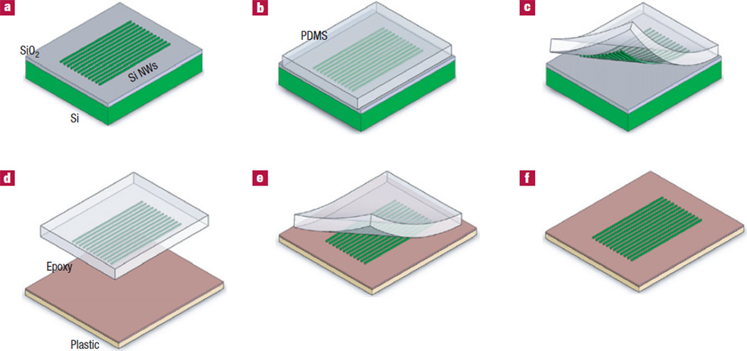
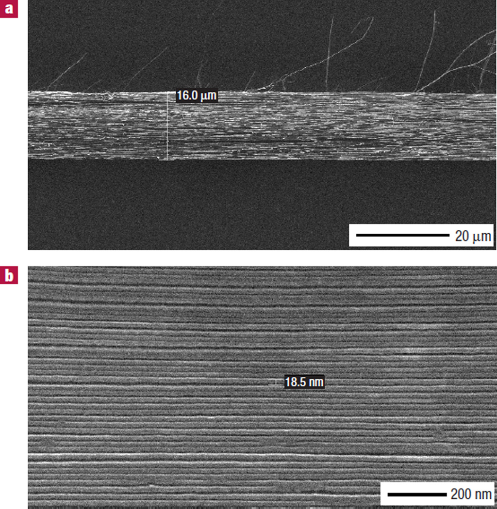
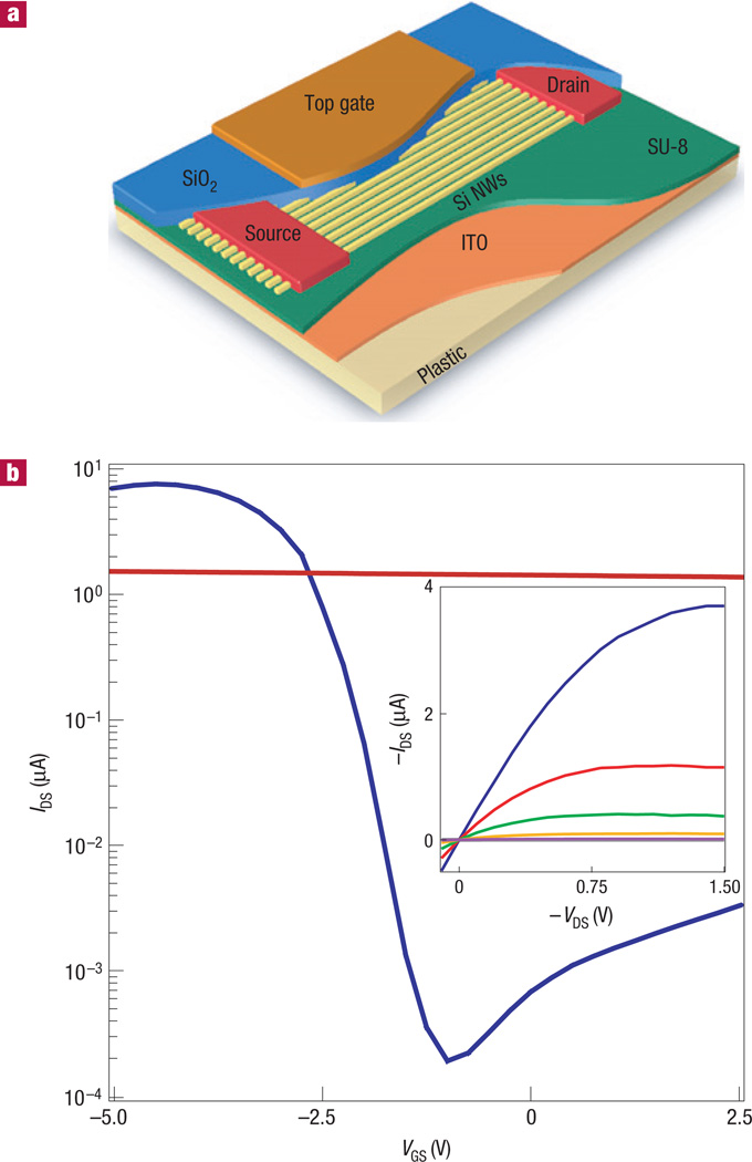
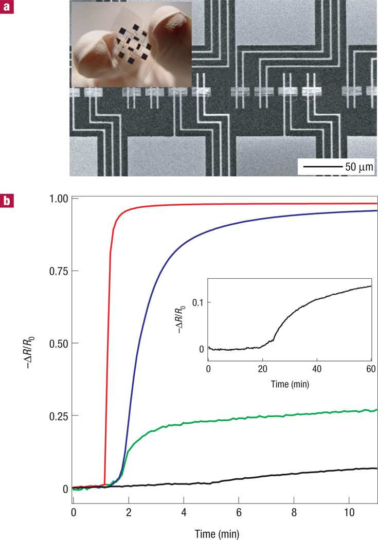
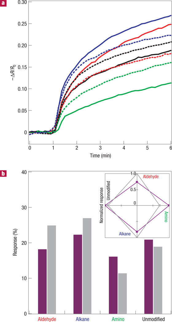
The development of a robust method for integrating high-performance semiconductors on flexible plastics could enable exciting avenues in fundamental research and novel applications. One area of vital relevance is chemical and biological sensing, which if implemented on biocompatible substrates, could yield breakthroughs in implantable or wearable monitoring systems. Semiconducting nanowires (and nanotubes) are particularly sensitive chemical sensors because of their high surface-to-volume ratios. Here, we present a scalable and parallel process for transferring hundreds of pre-aligned silicon nanowires onto plastic to yield highly ordered films for low-power sensor chips. The nanowires are excellent field-effect transistors, and, as sensors, exhibit parts-per-billion sensitivity to NO2, a hazardous pollutant. We also use SiO2 surface chemistries to construct a 'nano-electronic nose' library, which can distinguish acetone and hexane vapours via distributed responses. The excellent sensing performance coupled with bendable plastic could open up opportunities in portable, wearable or even implantable sensors.


Figures

Figure 1
Figure 1. Illustration of the steps for transfer printing SNAP nanowires onto plastic substrates
a, Nanowires are etched into a single-crystal silicon-on-insulator substrate. b, The exposed oxide is etched and a piece of PDMS makes conformal contact with the nanowire surfaces. c, The PDMS with adhered nanowires is peeled back from the host substrate. d, A plastic substrate is spin-cast with epoxy. e, The PDMS makes conformal contact with the plastic, and the epoxy is cured. f, Peeling back the PDMS leaves behind the SNAP nanowires in their original orientation, but on plastic.
Figure 2
Figure 2. Scanning electron micrographs of the SNAP nanowires on plastic
The submerged ITO layer acts as a charge sink for imaging. a, Low-magnification image of the transferred SNAP film consisting of about 400 wires. The total film width is indicated. b, High-magnification image. The diameter of a typical nanowire is indicated.
Figure 3
Figure 3. Electrical characterization of nanowire TFTs on plastic
a, Schematic illustration of the active area of a SNAP TFT, with the electrodes and various layers labelled. b, IDS versus VGS (VDS=1 V) for a multi-nanowire SNAP transistor. The red curve shows the response of the device when the voltage is applied to the backgate ITO. The blue curve shows the response when the voltage is applied to the top Ti gate electrode. The inset shows IDS versus VDS curves for the SNAP TFT on plastic. The blue, red, green, orange, purple and grey (overlapped by purple) curves correspond to VGS=−5, −4, −3, −2, −1 and 0 V, respectively, applied to the top-gate electrode.
Figure 4
Figure 4. Ultrasensitive detection with nanowire-on-plastic gas sensors
a, SEM image of an array of SNAP nanowire sensors. Each device (horizontal strip) is contacted by two Ti electrodes (oriented vertically) that extend to larger pads (top and bottom image edges). Inset: Digital photograph of the flexible sensor chip. b, Electrical response of a nanowire sensor to 20 p.p.m. (red curve), 2 p.p.m. (blue curve), 200 p.p.b. (green curve) and 20 p.p.b. (black curve) NO2 diluted in N2. The gas is introduced to the sensing chamber after 1 min of flowing N2. Inset: An extended response of the sensor to 20 p.p.b. NO2; the gas is introduced after 20 min of flowing N2.
Figure 5
Figure 5. Characterization of a ‘nano-electronic nose’ nanowire sensor library on plastic
a, The electrical response of a four-chemiresistor array to hexane vapour (solid lines) and acetone vapour (dashed lines). The vapours are introduced at time 1 min and allowed to flow for 5 min. The sensors are modified with alkane (blue), amino (green) and aldehyde (red) surface functionalities. One sensor (black) is unmodified. b, Bar graph summarizing the percentage change in response of the array to acetone (purple) and hexane (grey) vapours. The inset shows the normalized response of the sensor library to acetone and hexane vapours. Each of the four axes represents the four unique surface functionalities.

Similar articles

Cited by

References

    1. Service RF. Inorganic electronics begin to flex their muscle. Science. 2006;312:1593–1594. - PubMed
    1. Reuss RH, et al. Macroelectronics: Perspectives on technology and applications. Proc. IEEE. 2005;93:1239–1256.
    1. Xu JM. Plastic electronics and future trends in microelectronics. Synth. Met. 2000;115:1–3.
    1. Uchikoga S. Low-temperature polycrystalline silicon thin-film transistor technologies for system-on-glass displays. Mater. Res. Soc. Bull. 2002;27:881–885.
    1. Gosain DP, Noguchi T, Usui S. High mobility thin film transistors fabricated on a plastic substrate at a processing temperature of 110 °C. Jpn. J. Appl. Phys. 2000;39:L179–L181. 2.

Publication types

MeSH terms