. 2007 Jan 21;570(3):543-555.
doi: 10.1016/j.nima.2006.10.277.

A prototype of very high resolution small animal PET scanner using silicon pad detectors

Affiliations

A prototype of very high resolution small animal PET scanner using silicon pad detectors

Sang-June Park et al. Nucl Instrum Methods Phys Res A. .

Abstract

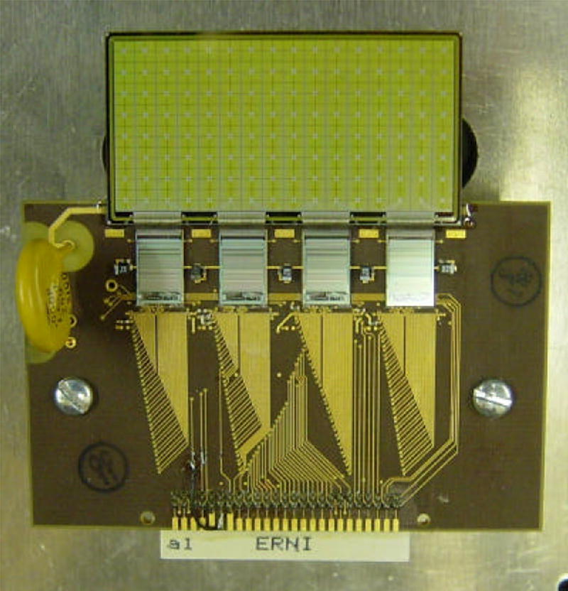
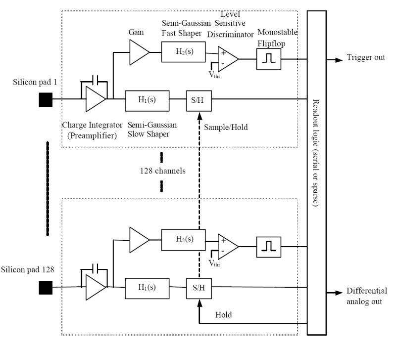
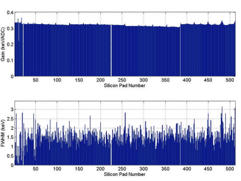
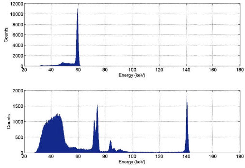
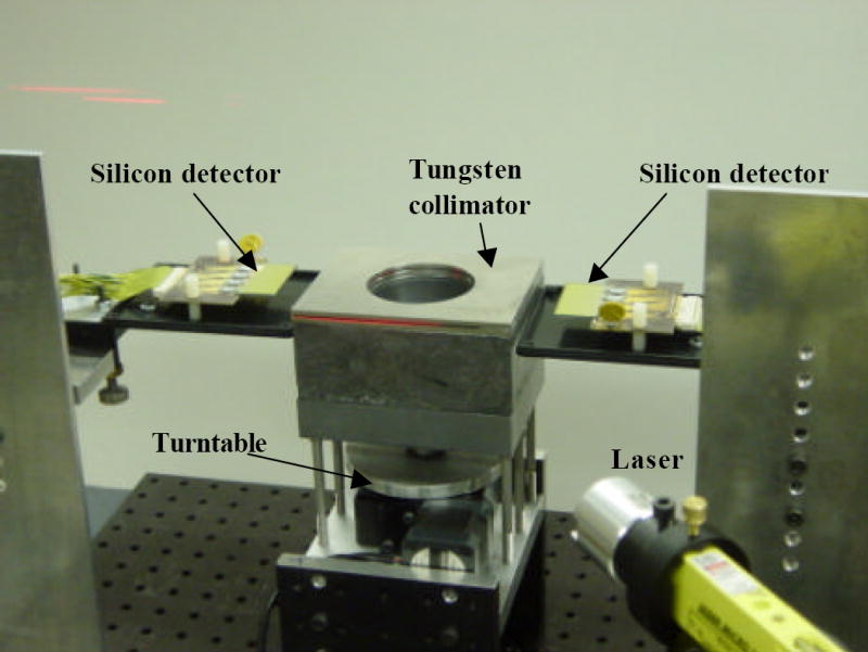
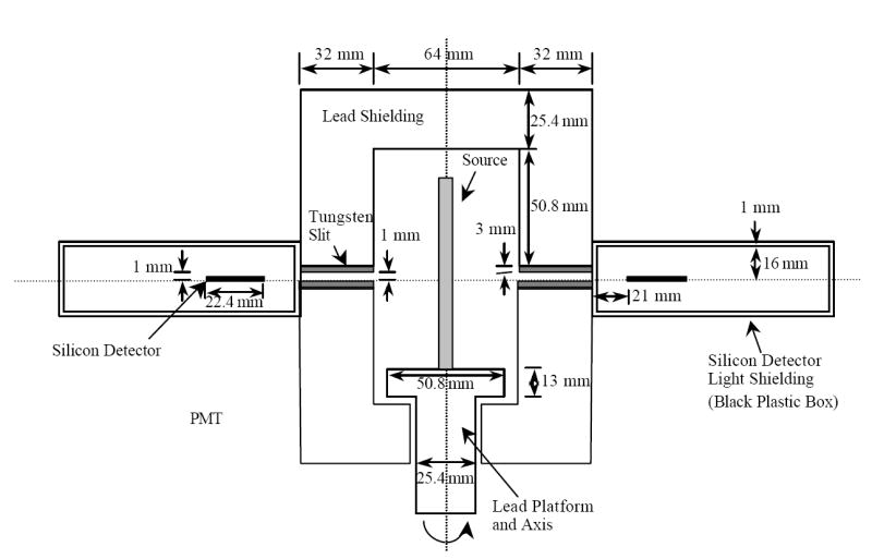
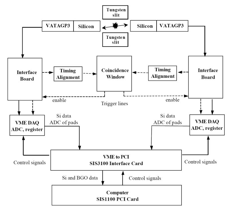
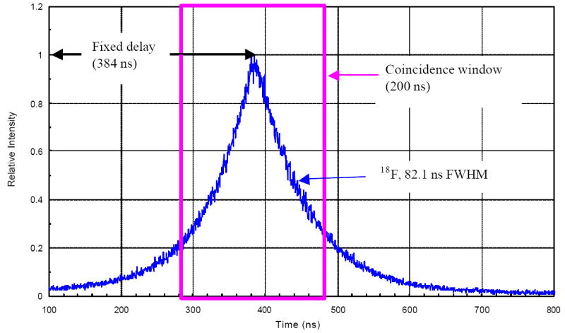
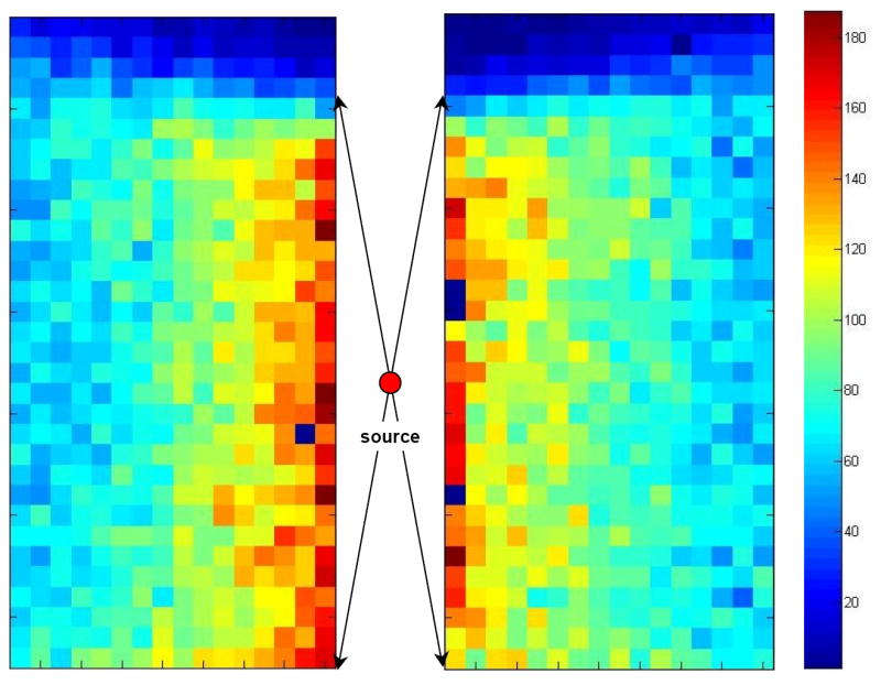
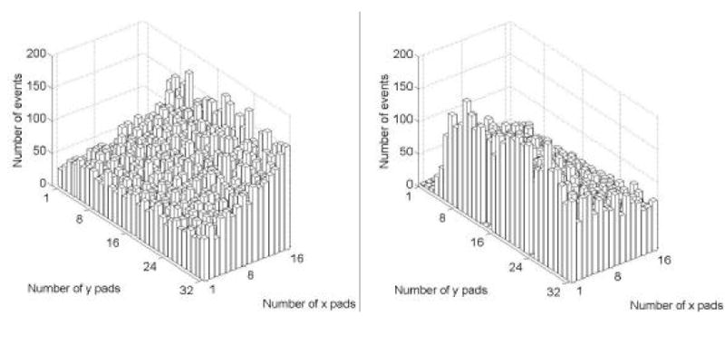
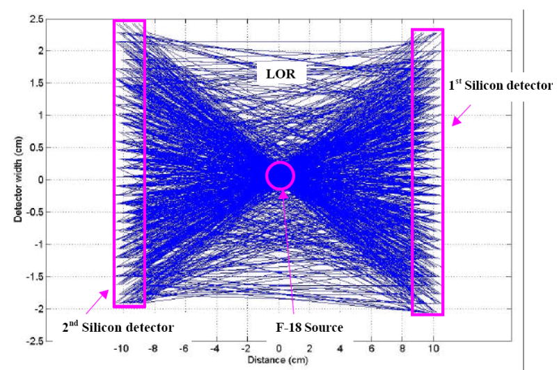
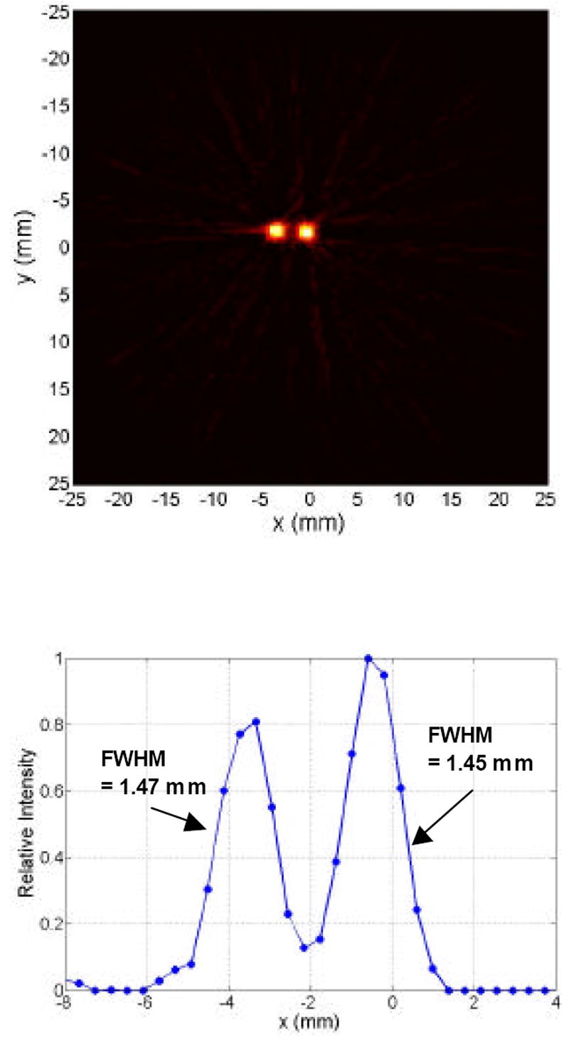
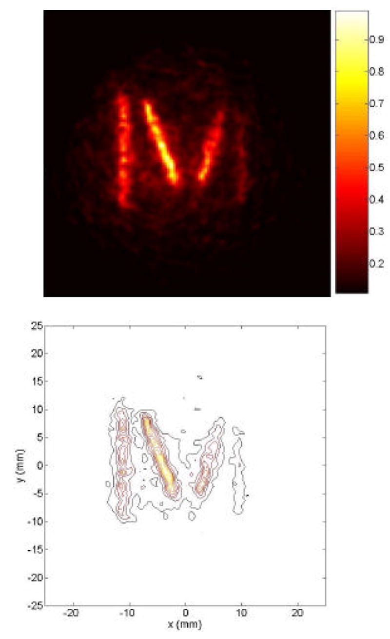
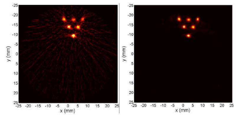
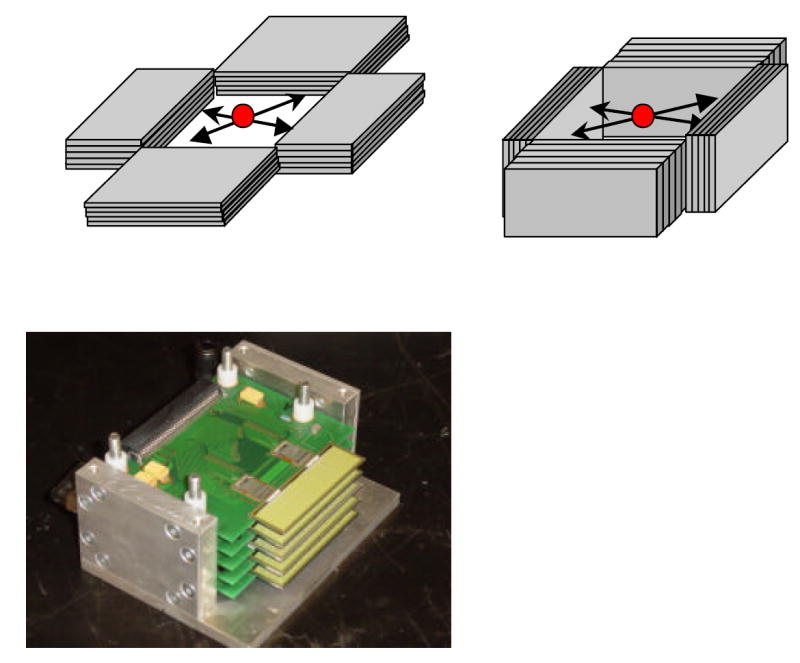
A very high resolution small animal positron emission tomograph (PET) which can achieve sub-millimeter spatial resolution is being developed using silicon pad detectors. The prototype PET for a single slice instrument consists of two 1 mm thick silicon pad detectors, each containing a 32 x 16 array of 1.4 mm x 1.4 mm pads read out with four VATAGP3 chips which have 128 channels low-noise self triggering ASIC in each chip, coincidence units, a source turntable and tungsten slice collimator. The silicon detectors were located edgewise on opposite sides of a 4 cm field-of-view to maximize efficiency. Energy resolution is dominated by electronic noise, which is 0.98% (1.38 keV) FWHM at 140.5 keV. Coincidence timing resolution is 82.1 ns FWHM and coincidence efficiency was measured to be 1.04 x 10(-3) % from two silicon detectors with annihilation photons of (18)F source Image data were acquired and reconstructed using conventional 2-D filtered-back projection (FBP) and a maximum likelihood expectation maximization (ML-EM) method. Image resolution of approximately 1.45 mm FWHM is obtained from 1-D profile of 1.1 mm diameter (18)F line source image. Even better resolution can be obtained with smaller detector element sizes. While many challenges remain in scaling up the instrument to useful efficiency including densely packed detectors and significantly improved timing resolution, performance of the test setup in terms of easily achieving submillimeter resolution is compelling.


Figures

Fig. 1
Fig. 1
Silicon pad sensor (32×16 array of 1.4 mm square pad and 1 mm thickness) manufactured by SINTEF and four VATAGP3 128-channel readout chips.
Fig. 2
Fig. 2
Block diagram of VATAGP3 readout chip.
Fig. 3
Fig. 3
Mean values (top) and standard deviations (bottom) of pedestals in ADC counts measured from the first silicon sensor.
Fig. 4
Fig. 4
Histograms of common mode noise from the first (left) and second (right) silicon detectors. The distributions are Gaussian-shaped with zero mean and 1.53 and 1.55 ADC FWHM from the first and second silicon detectors, respectively.
Fig. 5
Fig. 5
Gains (top) and pad-to-pad energy resolutions (bottom) from all channels of the first silicon sensor using 99mTc source.
Fig. 6
Fig. 6
Energy spectrum after gain correction from all 512 pads of the second silicon sensor with 241Am (top) and 99mTc (bottom). Energy resolutions are 1.45 keV FWHM at 59.5 keV of 241Am photopeak and 1.38 keV FWHM at 140.5 keV of 99mTc photopeak.
Fig. 7
Fig. 7
Photograph of the prototype PET consisting of two silicon pad detectors, a source turntable, lead shielding and tungsten collimator.
Fig. 8
Fig. 8
Cross-sectional view of the prototype setup.
Fig. 9
Fig. 9
Block diagram of the prototype system.
Fig. 10
Fig. 10
Coincidence timing spectrum from two silicon detectors of the prototype setup using 18F source. Timing resolution is 82.1 ns FWHM.
Fig. 11
Fig. 11
2-D plot of the number of coincidence events in each pad or hit map from the first (right) and second (left) silicon detectors. The source is located at few millimeters below from the center of FOV.
Fig. 12
Fig. 12
3-D plot of the number of coincidence events in each pad or hit map from the first (right) and second (left) silicon detectors.
Fig. 13
Fig. 13
LOR plot from 1000 coincidence events using the first (right) and second (left) silicon detectors.
Fig. 14
Fig. 14
Two line source image from 18F-FDG in two glass capillary tubes (1.1-1.2 mm I.D.). The gap between two sources is 2.0 mm. 2-D FBP with a ramp filter having a cutoff at the Nyquist frequency was used to reconstruct image. (Top): 2-D image. (Bottom): 1-D profile of the 2-D image.
Fig. 15
Fig. 15
Five line source image reconstructed with 2-D FBP with ramp filter. The source (18F-FDG in glass capillary tubes) located at r = 0, 2, 5, 10, and 20 mm from the FOV.
Fig. 16
Fig. 16
2-D (top) and contour (bottom) images reconstructed with a ML-EM (30 iterations) using four 18F line sources in “M” shape. The size of each image is 5 cm × 5 cm.
Fig. 17
Fig. 17
Six line source images reconstructed with 2-D FBP (left) with a ramp filter having a cutoff at the Nyquist frequency and 2-D ML-EM (right) with 20 iterations. Attenuation, scatter, and random were not corrected in the both images. 18F-FDG was filled in 1.1 mm diameter hot rods of resolution phantom (a Lucite cylinder with a 4.4 cm diameter and 3.4 cm height). Center-to-center spacing of hot rods is 5 mm.
Fig. 18
Fig. 18
(Bottom): A stack of silicon module. (Top): Detector arrangements used in a multi-slice PET scanner design using four silicon modules.

References

    1. Yang Y, et al. Phys Med Biol. 2004;49:2527. - PubMed
    1. Tai Y, et al. Phys Med Biol. 2003;48:1519. - PubMed
    1. Stickel JR, Cherry SR. Phys Med Biol. 2005;50:179. - PubMed
    1. Clinthorne NH, et al. J Nucl Med Suppl. 2000;41:20.
    1. Park S, et al. J Nucl Med Suppl. 2001;42:55.

LinkOut - more resources