

doi: 10.1126/science.1162193.
Epub 2008 Aug 14.
Polymer pen lithography
Affiliations
- PMID: 18703709
- PMCID: PMC8247121
- DOI: 10.1126/science.1162193
Item in Clipboard
Polymer pen lithography
Science.
.
Abstract
We report a low-cost, high-throughput scanning probe lithography method that uses a soft elastomeric tip array, rather than tips mounted on individual cantilevers, to deliver inks to a surface in a "direct write" manner. Polymer pen lithography merges the feature size control of dip-pen nanolithography with the large-area capability of contact printing. Because ink delivery is time and force dependent, features on the nanometer, micrometer, and macroscopic length scales can be formed with the same tip array. Arrays with as many as about 11 million pyramid-shaped pens can be brought into contact with substrates and readily leveled optically to ensure uniform pattern development.
Figures
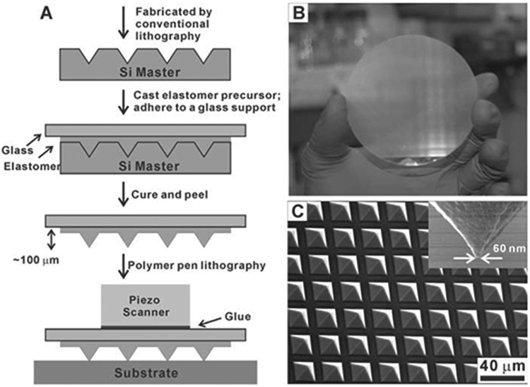
(A) A schematic illustration of the polymer pen lithography setup. (B) A photograph of an 11-million-pen array. (C) Scanning electron microscope image of the polymer pen array. The average tip radius of curvature is 70 ± 10 nm (inset).
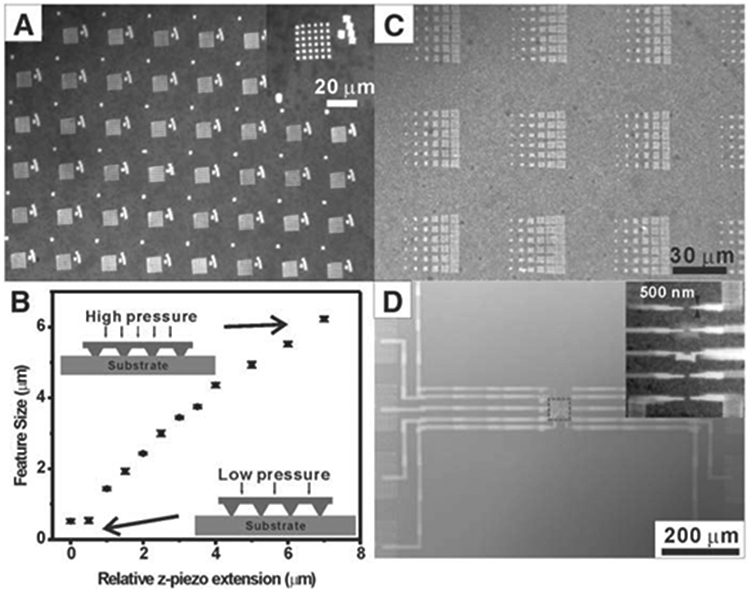
(A) Optical image of a 480-μm by 360-μm section of a one million gold dot array (6 by 6 within each block) on a silicon substrate (using a pen array with 28,000 pyramid-shaped tips). (B) MHA dot size as a function of relative z-piezo extension. The results were obtained using a polymer pen array with 15,000 pyramid-shaped tips at 25°C with a relative humidity of 40%. (C) Optical image of arrays of gold squares generated at different z-piezo extensions (using a pen array with 28,000 pyramid-shaped tips). (D) An optical microscope image of a multidimensional gold circuit fabricated by PPL. The inset shows a magnified SEM image of the circuit center.
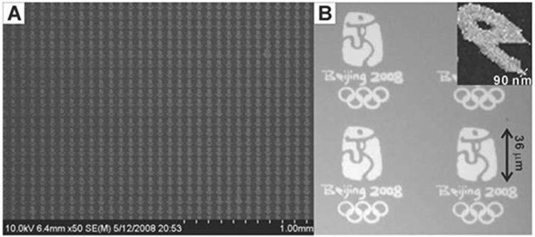
(A) SEM image of a representative region of ~15,000 miniaturized duplicates of the 2008 Beijing Olympic logo. (B) A zoom-in optical image of a representative replica. The inset shows a magnified SEM image of the letter “e.”
Similar articles
-
Hard Transparent Arrays for Polymer Pen Lithography.ACS Nano. 2016 Mar 22;10(3):3144-8. doi: 10.1021/acsnano.6b00528. Epub 2016 Mar 1. ACS Nano. 2016. PMID: 26928012 Free PMC article.
-
"Force-feedback" leveling of massively parallel arrays in polymer pen lithography.Nano Lett. 2010 Apr 14;10(4):1335-40. doi: 10.1021/nl904200t. Nano Lett. 2010. PMID: 20184292 Free PMC article.
-
Beam pen lithography.Nat Nanotechnol. 2010 Sep;5(9):637-40. doi: 10.1038/nnano.2010.161. Epub 2010 Aug 1. Nat Nanotechnol. 2010. PMID: 20676088
-
Strategies for patterning biomolecules with dip-pen nanolithography.Small. 2011 Apr 18;7(8):989-1002. doi: 10.1002/smll.201001749. Epub 2011 Mar 14. Small. 2011. PMID: 21400657 Review.
-
Molecular printing.Nat Chem. 2009 Aug;1(5):353-8. doi: 10.1038/nchem.258. Epub 2009 Jun 28. Nat Chem. 2009. PMID: 21378889 Free PMC article. Review.
Cited by
-
Micro-to-nanometer patterning of solution-based materials for electronics and optoelectronics.RSC Adv. 2019 Nov 22;9(65):38085-38104. doi: 10.1039/c9ra07514c. eCollection 2019 Nov 19. RSC Adv. 2019. PMID: 35541771 Free PMC article. Review.
-
Nanobiochips.Cell Mol Life Sci. 2012 Feb;69(3):347-56. doi: 10.1007/s00018-011-0853-9. Epub 2011 Nov 1. Cell Mol Life Sci. 2012. PMID: 22042270 Free PMC article. Review.
-
A Versatile Microarray Platform for Capturing Rare Cells.Sci Rep. 2015 Oct 23;5:15342. doi: 10.1038/srep15342. Sci Rep. 2015. PMID: 26493176 Free PMC article.
-
Dip-Pen Nanolithography(DPN): from Micro/Nano-patterns to Biosensing.Chem Res Chin Univ. 2021;37(4):846-854. doi: 10.1007/s40242-021-1197-0. Epub 2021 Jul 5. Chem Res Chin Univ. 2021. PMID: 34376961 Free PMC article. Review.
-
Low-cost fabrication of centimetre-scale periodic arrays of single plasmid DNA molecules.Lab Chip. 2013 Sep 7;13(17):3367-72. doi: 10.1039/c3lc50562f. Epub 2013 Jul 4. Lab Chip. 2013. PMID: 23824041 Free PMC article.
References
-
- Mirkin CA, ACS Nano 1, 79 (2007). - PubMed
-
- Salaita K, Wang YH, Mirkin CA, Nat. Nanotechnol 2, 145 (2007). - PubMed
-
- Ginger DS, Zhang H, Mirkin CA, Angew. Chem. Int. Ed 43, 30 (2004). - PubMed
-
- Xia Y, Whitesides GM, Angew. Chem. Int. Ed 37, 550 (1998). - PubMed
-
- Xia Y, Whitesides GM, Annu. Rev. Mater. Sci 28, 153 (1998).
Publication types
MeSH terms
Substances
Grants and funding
LinkOut - more resources
Full Text Sources
Other Literature Sources
