. 2008;55(7):1863-1872.
doi: 10.1109/TCSI.2008.918006.

A Charge-Based Low-Power High-SNR Capacitive Sensing Interface Circuit

A Charge-Based Low-Power High-SNR Capacitive Sensing Interface Circuit

Sheng-Yu Peng et al. IEEE Trans Circuits Syst I Regul Pap. 2008.

Abstract

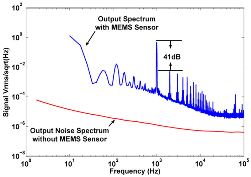
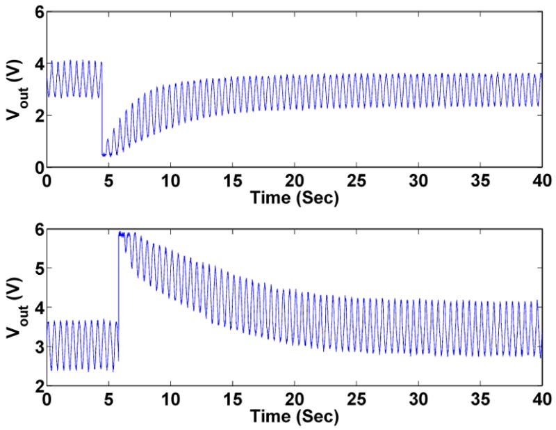
This paper describes a low-power approach to capacitive sensing that achieves a high signal-to-noise ratio. The circuit is composed of a capacitive feedback charge amplifier and a charge adaptation circuit. Without the adaptation circuit, the charge amplifier only consumes 1 μW to achieve the audio band SNR of 69.34dB. An adaptation scheme using Fowler-Nordheim tunneling and channel hot electron injection mechanisms to stabilize the DC output voltage is demonstrated. This scheme provides a very low frequency pole at 0.2Hz. The measured noise spectrums show that this slow-time scale adaptation does not degrade the circuit performance. The DC path can also be provided by a large feedback resistance without causing extra power consumption. A charge amplifier with a MOS-bipolar pseudo-resistor feedback scheme is interfaced with a capacitive micromachined ultrasonic transducer to demonstrate the feasibility of this approach for ultrasound applications.


Figures

Fig. 1
Fig. 1. Capacitive sensing diagrams
(a) In a typical two-chip hybrid approach, the small variance of the sensing capacitor, ΔC, the large parasitic capacitance, Cw, and the static capacitance, Csensor, as well as the leakage currents at the interconnect make the sensing circuit design a challenge. (b) A new approach to sensing capacitive change by using a charge amplifier with a charge adaptation circuit.
Fig. 2
Fig. 2. Capacitive circuits
(a) A capacitive voltage divider. (b) A capacitive feedback amplifier. (c)A capacitive feedback amplifier for capacitive sensing.
Fig. 3
Fig. 3. Schematics of small signal models and a cascode OTA
(a) The small-signal model of the capacitive sensing circuit. (b) A single-stage cascode operational transconductance amplifier. (c) The small-signal model of (a) for noise analysis. (d) The simplified small-signal model from (b) for noise analysis.
Fig. 4
Fig. 4. Measured waveform
The input music waveform and the recorded waveform from a capacitive feedback amplifier. The distortion comes from the nonlinearity of the speaker, the background 60Hz noise, the offset of the OTA, and the limitation of the supply rails.
Fig. 5
Fig. 5. Nonlinearity of an OTA
The relation between the total harmonic distortion (THD) and the maximum input linear voltage of a differential pair in the subthreshold region. The total harmonic distortion is calculated from (10) with UT = 25 mV and κ = 0.7
Fig. 6
Fig. 6. The setup for audio measurements and the micrographs
(a) Setup of the capacitive sensing measurement. The charge adaptation circuitry is disabled by connecting the tunneling and the drain voltages to 3.3V. The non-inverting terminal voltage is adjusted so that the output voltage is at the mid-rail. (b) A die micrograph of a version of the capacitive feedback amplifier fabricated in a 0.5 μm double-poly CMOS process. (c) A micrograph of the MEMS sensor used in the measurement.
Fig. 7
Fig. 7. The measured output signal and noise spectrums
A card type speaker is used as the 1K Hz acoustic signal source and a MEMS microphone is interfaced with the circuit. -38dB THD is observed when the output is 1Vrms.
Fig. 8
Fig. 8. Noise spectrums of a charge amplifier with a linear input capacitor
The circuit is connected to a linear 2 pF capacitor. The tail current of the OTA amplifier is tunable and the corresponding power consumptions of the three noise spectrums are 1 μW, 0.23 μW, and 0.13uW respectively. The bandwidth increases as the power increases but the total output noise remains constant. The noise in the audio band can be reduced by consuming more power if the circuit is followed by a low-pass filter.
Fig. 9
Fig. 9. Setup for the measurement with charge adaptation scheme
A an indirect injection transistor and a tunneling junction are integrated on chip. A comparator composed of discrete transistors provides the drain voltage of the injection transistor so that the injection current can balance out the tunneling and the leakage currents.
Fig. 10
Fig. 10. Adaptation step responses
Steps from 0V to 5V and from 5V to 0V are applied to the biased terminal of the sensor. The output voltage is adapted to the mid-rail by the injection and the tunneling mechanisms.
Fig. 11
Fig. 11. Noise spectrum comparison
Using the tunneling and the injection mechanisms to autozero the output voltage does not affect the noise performance of the circuit over the frequency band of interest. Both spectrums are measured with audio MEMS sensor.
Fig. 12
Fig. 12. Setup for the ultrasonic measurement
A capacitive sensing circuit is connected to a CMUT device. MOS-bipolar pseudo-resistor feedback scheme is used to stabilize the output DC voltage.
Fig. 13
Fig. 13. Measured waveform from an ultrasonic transducer
The measured waveform from a charge amplifier that is connected to a CMUT device with a MOS-bipolar pseudo-resistor feedback scheme. The first acoustic signal arrives 15 microseconds after the piezo transducer is activated.
Fig. 14
Fig. 14. Previous approaches to capacitive sensing
(a) Switched-capacitor approach. (b) Lock-in approach. (c) A self-biased JFET buffer as a microphone interface circuit. (d) The current through JFET is sensed and amplified to improve PSRR. (e)-(h) Diodes or linearized OTA are used as a large resistor and the voltage is directly amplified or buffered and then amplified.

References

    1. Kucic M, Low A, Hasler P, Neff J. A programmable continuous-time floating-gate Fourier processor. IEEE Trans Circuit and system II. 2001 Jan;:90–99.
    1. Hasler P, Minch BA, Diorio C. An autozeroing floating-gate amplifier. IEEE Trans Circuit and system II. 2001 Jan;48(1):74–82.
    1. Ramirez-Angulo J, Lopez-Martin AJ, Carvajal RG, Chavero FM. Very low-voltage analog signal processing based on quasi-floating gate transistors. J SOLID-STATE CIRCUITS. 2004 June;39(3)
    1. Peng S-Y, Qureshi MS, Hasler PE, Hall NA, Degertekin FL. High signal-to-noise ratio capacitive sensing transducer. IEEE Proceedings of the International Symposium on Circuits and Systems. 2006 May;
    1. Peng S-Y, Qureshi MS, Basu A, Hasler PE, Degertekin FL. A floating-gate based low-power capacitive sensing interface circuit. IEEE Proceedings of the Custom Integrated Circuits Conference. 2006 Sep;

LinkOut - more resources