. 2008 Dec 2;105(48):18675-80.
doi: 10.1073/pnas.0807476105. Epub 2008 Nov 17.

Materials and noncoplanar mesh designs for integrated circuits with linear elastic responses to extreme mechanical deformations

Affiliations

Materials and noncoplanar mesh designs for integrated circuits with linear elastic responses to extreme mechanical deformations

Dae-Hyeong Kim et al. Proc Natl Acad Sci U S A. .

Abstract

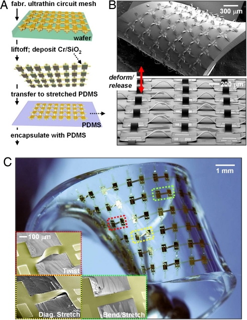
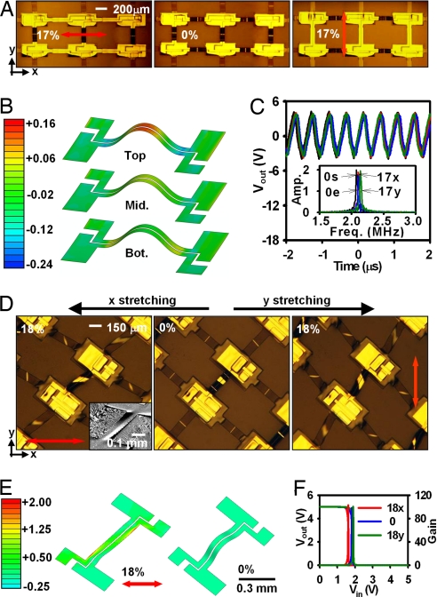
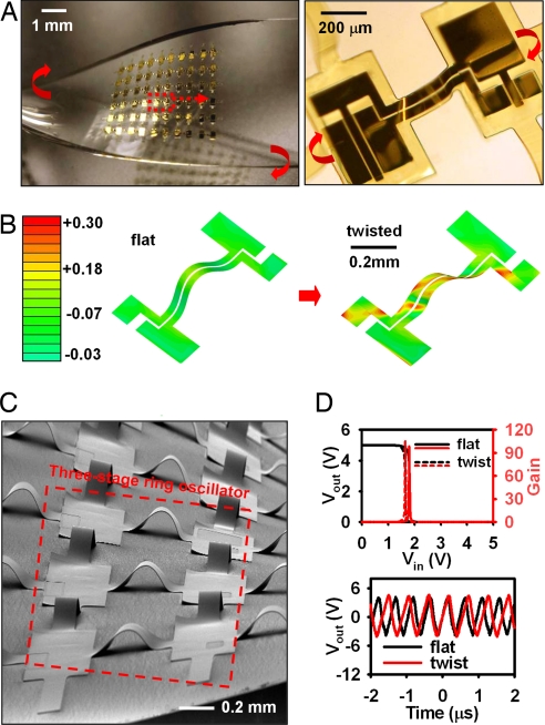
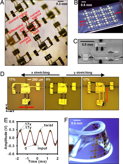
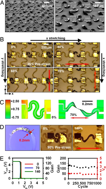
Electronic systems that offer elastic mechanical responses to high-strain deformations are of growing interest because of their ability to enable new biomedical devices and other applications whose requirements are impossible to satisfy with conventional wafer-based technologies or even with those that offer simple bendability. This article introduces materials and mechanical design strategies for classes of electronic circuits that offer extremely high stretchability, enabling them to accommodate even demanding configurations such as corkscrew twists with tight pitch (e.g., 90 degrees in approximately 1 cm) and linear stretching to "rubber-band" levels of strain (e.g., up to approximately 140%). The use of single crystalline silicon nanomaterials for the semiconductor provides performance in stretchable complementary metal-oxide-semiconductor (CMOS) integrated circuits approaching that of conventional devices with comparable feature sizes formed on silicon wafers. Comprehensive theoretical studies of the mechanics reveal the way in which the structural designs enable these extreme mechanical properties without fracturing the intrinsically brittle active materials or even inducing significant changes in their electrical properties. The results, as demonstrated through electrical measurements of arrays of transistors, CMOS inverters, ring oscillators, and differential amplifiers, suggest a valuable route to high-performance stretchable electronics.


Conflict of interest statement

The authors declare no conflict of interest.

Figures

Fig. 1.
Fig. 1.
Fabrication of noncoplanar stretchable electronics and responses to deformation. (A) Schematic overview of the fabrication process for representative circuits that accomplish high levels of stretchability through the use of noncoplanar mesh designs integrated with elastomeric substrates [for the case shown here, PDMS]. (B) SEM images of an array of CMOS inverters that result from this process, in an undeformed state (Lower; ≈20% prestrain) and in a corresponding configuration that results from a complex twisting motion (Upper). (C) Optical image of a freely deformed stretchable array of CMOS inverters, highlighting 3 different classes of deformation: diagonal stretching, twisting, and bending. The Insets provide SEM images for each case (colorized for ease of viewing).
Fig. 2.
Fig. 2.
Mechanical and electrical responses of noncoplanar stretchable electronics to in-plane strains. (A) Optical images of stretchable, 3-stage CMOS ring oscillators with noncoplanar mesh designs, for stretching along the bridges (x and y). (B) FEM modeling of the strain distributions at the top surface of the circuit (Top) and at the midpoint of the metal layer (Mid.) and bottom surface (Bot.). (C) Electrical characteristics of the oscillators as represented in the time and frequency (Inset) domains in the different strain configurations illustrated in A. Here, 0s and 0e refer to 0% strains at the start and end of the testing, respectively; 17x and 17y refer to 17% tensile strains along the x and y directions indicated in A, respectively. (D) Optical images of stretchable CMOS inverters with noncoplanar mesh designs, for stretching at 45° to the directions of the bridges (x and y). (E) FEM simulations of these motions. (F) Transfer characteristics of the inverters (output voltage, Vout, and gain as a function of input voltage, Vin). The notations 18x and 18y refer to 18% tensile strains along the x and y directions indicated in D, respectively.
Fig. 3.
Fig. 3.
Mechanical and electrical responses of noncoplanar stretchable electronics to twisting deformations. (A) Optical images of an array of stretchable CMOS inverters in a twisted configuration (Left) and magnified view of a single inverter, illustrating the nature of the deformation (Right). (B) FEM simulation of the mechanics of twisting on the bridge structures. (C) SEM image of an array of stretchable, 3-stage CMOS ring oscillators in a twisted configuration. (D) Electrical characteristics of the inverters (Upper; gain and output voltage, Vout, as a function of input voltage, Vin) and oscillators (Lower; output voltage, Vout, as a function of time) in planar and twisted states.
Fig. 4.
Fig. 4.
Noncoplanar stretchable electronics with asymmetric layouts. (A and B) Optical images of an array of stretchable differential amplifiers in twisted (A) and planar stretched (B) layouts. (C) Tilted view SEM of a representative amplifier, showing the noncoplanar layout. (D and E) Optical images under stretching along the x and y directions (D) and corresponding electrical output as a function of time for a sinusoidal input (E). (F) Optical image of a device in a complex deformation mode. Here, 17x and 17y refer to 17% tensile strains along the x and y directions indicated in D, respectively.
Fig. 5.
Fig. 5.
Extreme stretchability in noncoplanar electronics with serpentine bridge designs. (A) SEM image of an array of stretchable CMOS inverters with noncoplanar bridges that have serpentine layouts (Left) and magnified view (Right). (B) Optical images of stretching tests in the x and y directions. (C) FEM simulation before (35% prestrain) and after (70% applied strain) stretching. (D) Arrays of inverters on a thin PDMS substrate (0.2 mm) (Left) and images in unstretched (middle; 90% prestrain) and stretched (Right; 140% tensile strain) states. (E) Transfer characteristics and gain for a representative inverter under stretching (Left) and plot of gain and voltage at maximum gain (VM) for a similar device as a function of stretching cycles (Right).

References

    1. Reuss RH, et al. Macroelectronics: Perspectives on technology and applications. Proc IEEE. 2005;93:1239–1256.
    1. Reuss RH, et al. Macroelectronics. MRS Bull. 2006;31:447–454.
    1. Lacour SP, Jones J, Wagner S, Li T, Suo Z. Stretchable interconnects for elastic electronic surfaces. Proc IEEE. 2005;93:1459–1467.
    1. Kim D-H, et al. Stretchable and foldable silicon integrated circuits. Science. 2008;320:507–511. - PubMed
    1. Someya T, et al. Conformable, flexible, large-area networks of pressure and thermal sensors with organic transistor active matrixes. Proc Natl Acad Sci USA. 2005;102:12321–12325. - PMC - PubMed

Publication types

LinkOut - more resources