. 2009 Jan;4(1):56-63.
doi: 10.1038/nnano.2008.360. Epub 2008 Dec 7.

Tuning the optical and electronic properties of colloidal nanocrystals by lattice strain

Affiliations

Tuning the optical and electronic properties of colloidal nanocrystals by lattice strain

Andrew M Smith et al. Nat Nanotechnol. 2009 Jan.

Abstract

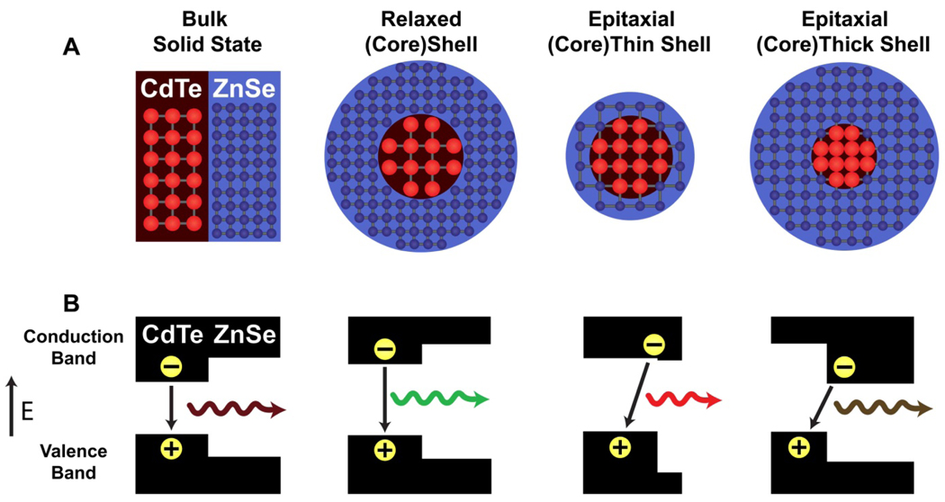
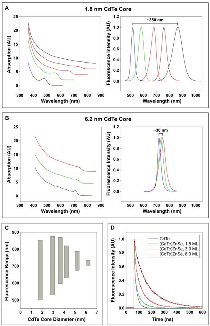
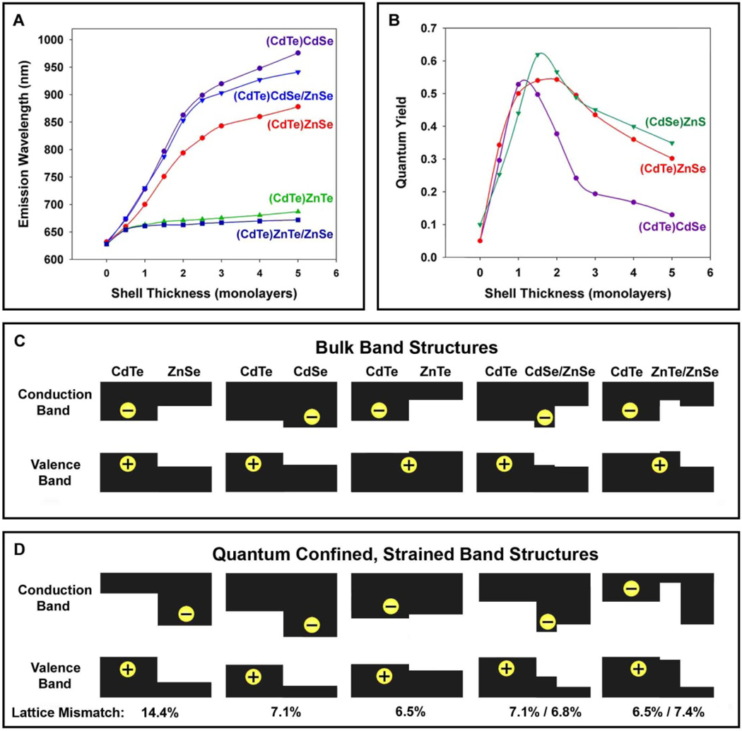
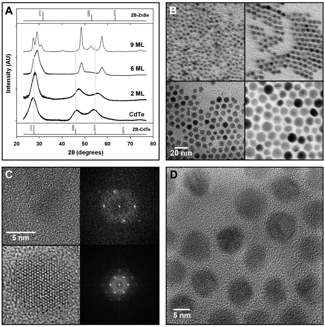
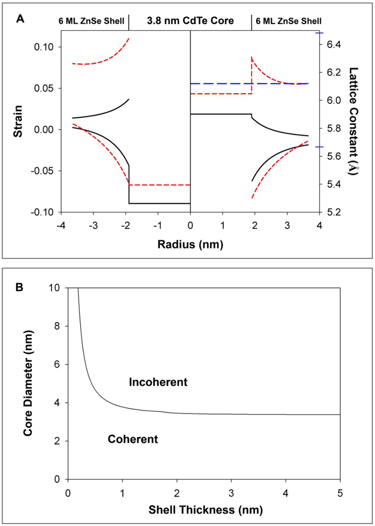
Strain can have a large influence on the properties of materials at the nanoscale. The effect of lattice strain on semiconductor devices has been widely studied, but its influence on colloidal semiconductor nanocrystals is still poorly understood. Here we show that the epitaxial deposition of a compressive shell (ZnS, ZnSe, ZnTe, CdS or CdSe) onto a soft nanocrystalline core (CdTe) to form a lattice-mismatched quantum dot can dramatically change the conduction and valence band energies of both the core and the shell. In particular, standard type-I quantum-dot behaviour is replaced by type-II behaviour, which is characterized by spatial separation of electrons and holes, extended excited-state lifetimes and giant spectral shifts. Moreover, the strain induced by the lattice mismatch can be used to tune the light emission--which displays narrow linewidths and high quantum yields--across the visible and near-infrared part of the spectrum (500-1,050 nm). Lattice-mismatched core-shell quantum dots are expected to have applications in solar energy conversion, multicolour biomedical imaging and super-resolution optical microscopy.


Figures

Figure 1
Figure 1. Schematic illustration of band energy changes in semiconductor quantum dots induced by lattice strain
(A) Lattice structures of ordinary and strained (CdTe)ZnSe heterojunctions. From left to right: bulk (CdTe)ZnSe marterial, a relaxed (CdTe)ZnSe dot, a strained CdTe core with a markedly “stretched” ZnSe shell (thin), and a markedly “squeezed” CdTe core with a strained ZnSe shell (thick). (B) Valence and conduction band energy levels corresponding to bulk, relaxed, and strained (CdTe)ZnSe heterostructures in (A). Note that relaxed (CdTe)ZnSe nanostructures are standard type-I QDs, but are converted into type-II behavior when both the core and shell are strained by epitaxial growth. The electrons and holes are colocalized in type-I QDs, whereas they are spatially separated into the shell and the core in type-II QDs (see text for discussion). Discrete electronic energy levels caused by quantum confinement are omitted for simplicity. The impact of strain on band structures is calculated by using the model-solid theory and a continuum elasticity model (see Methods).
Figure 2
Figure 2. Optical properties of strain-tuned QDs with different CdTe core sizes (1.8 – 6.2 nm) and shell thicknesses (0 – 5 ZnSe monolayers)
(A) Absorption (left) and fluorescence emission (right) spectra of (CdTe)ZnSe QDs with 1.8 nm CdTe cores (blue), and capped with 0.5 (green), 1.0 (red), 3.0 (brown), or 6.0 (black) monolayers of ZnSe shell. The thickness of one monolayer of ZnSe is 2.83 angstroms. (B) Absorption (left) and fluorescence emission (right) spectra of (CdTe)ZnSe QDs with 6.2 nm CdTe cores (blue), and capped with 2.0 (green) and 5.0 (red) monolayers of ZnSe shell. (C) Strain-tunable spectral ranges for different CdTe core sizes, as measured by the fluorescence emission peaks with 0–5 monolayers of shell growth. Epitaxial growth on cores larger than 6.2 nm was not successful. (D) Time-resolved fluorescence decay curves of 3.8 nm CdTe QDs with 0 (blue), 1.5 (green), 3.0 (red), or 6.0 (brown) monolayers of ZnSe shell. The excited state lifetimes were calculated to be 18.4, 35.5, 59.8, and 115.0 ns, respectively. A pulsed 478 nm diode laser was used for excitation.
Figure 3
Figure 3. Comparison of emission wavelengths and fluorescence quantum yields for CdTe cores coated with different shell materials and thicknesses
(A) Emission wavelengths of 3.8 nm CdTe cores capped with ZnSe, CdSe, or ZnTe, or one monolayer of ZnTe followed by ZnSe (ZnTe/ZnSe), or one monolayer of CdSe followed by ZnSe (CdSe/ZnSe). (B) Fluorescence quantum yields of 3.8 nm CdTe cores capped with either ZnSe or CdSe, and CdSe QDs (3.8 nm) capped with ZnS for different shell thicknesses. (C) Diagrams of band offsets for core/shell nanocrystals in (A), as calculated by using the model-solid theory and a continuum elasticity model for the impact of strain (see Methods).
Figure 4
Figure 4. Lattice structures of strain-tunable QDs as determined by power x-ray diffraction and high-resolution transmission electron microscopy
(A) Powder x-ray diffraction patterns for 3.8 nm CdTe QDs, and (CdTe)ZnSe QDs with 2, 6, or 9 monolayers of shell growth, from bottom to top. Bulk diffraction peaks for zinc blende (ZB) CdTe and ZnSe are indexed at the bottom and top, respectively, and vertical lines correspond to the major diffraction lines of CdTe. The x-ray wavelength was 1.78897 Å. (B) Transmission electron micrographs of 3.8 nm CdTe cores capped with 0 (top left), 2 (top right), 6 (bottom left), and 9 (bottom right) monolayers of ZnSe. (C) High-resolution transmission electron micrographs of 3.8 nm CdTe QDs (top) and (CdTe)ZnSe QDs with 6 monolayers of shell (bottom). Fast-Fourier transform spectra of these materials are shown on the right. (D) HRTEM of (CdTe)ZnSe QDs with 6 monolayers of shell, showing all QDs to be oriented with the (001) lattice plane parallel to the substrate. The absorption and emission spectra of these (core)shell QDS are provided in Supplementary Figure 4, and their simulated diffraction and particle size distribution data are shown in Supplementary Figures 4 and 5. The results obtained from a line-wdith analysis of the diffraction peaks are summarized in Supplementary Table 1.
Figure 5
Figure 5. Theoretical predictions of high strain (CdTe)ZnSe QDs from a continuum elasticity model
(A) Left axis: strain distribution in 3.8 nm-diameter CdTe nanocrystals capped with 6 monolayers of ZnSe shell. The solid black line indicates strain for the QDs modeled as concentric spheres, and the red hatched lines as concentric cylinders. Strain within the core is compressive and isotropic, while the strain in the shell is compressive in the radial direction (bottom line) and tensile in the tangential direction (top line). Right axis: Calculated lattice constants corresponding to strain profiles for strained, concentric, core/shell spheres and cylinders. The blue hatched line shows the observed lattice constant, determined from XRD and TEM. Blue indices on the axis depict the bulk lattice constants of CdTe (6.482 Å) and ZnSe (5.6676 Å). (B) The critical thickness (black line) is the shell thickness for which the formation of a dislocation loop is energetically more favorable than coherent, epitaxial growth for different core sizes and shell thicknesses.

Comment in

References

    1. Robinson RD, et al. Spontaneous superlattice formation in nanorods through partial cation exchange. Science. 2007;317:355–358. - PubMed
    1. Lee J, et al. Bandgap modulation of carbon nanotubes by encapsulated metallofullerenes. Nature. 2002;415:1005–1008. - PubMed
    1. Suhr J, et al. Fatigue resistance of aligned carbon nanotube arrays under cyclic compression. Nature Nanotech. 2007;2:417–421. - PubMed
    1. Hall AR, Falvo MR, Superfine R, Washburn S. Electromechanical response of single-walled carbon nanotubes to torsional strain in a self-contained device. Nature Nanotech. 2007;2:413–416. - PubMed
    1. Roberts MM, et al. Elastically relaxed free-standing strained-silicon nanomembranes. Nature Mater. 2006;5:388–393. - PubMed

Publication types

LinkOut - more resources