. 2009 Sep 8;106(36):15254-8.
doi: 10.1073/pnas.0906943106. Epub 2009 Aug 24.

Diameter-dependent dopant location in silicon and germanium nanowires

Affiliations

Diameter-dependent dopant location in silicon and germanium nanowires

Ping Xie et al. Proc Natl Acad Sci U S A. .

Abstract

We report studies defining the diameter-dependent location of electrically active dopants in silicon (Si) and germanium (Ge) nanowires (NWs) prepared by nanocluster catalyzed vapor-liquid-solid (VLS) growth without measurable competing homogeneous decomposition and surface overcoating. The location of active dopants was assessed from electrical transport measurements before and after removal of controlled thicknesses of material from NW surfaces by low-temperature chemical oxidation and etching. These measurements show a well-defined transition from bulk-like to surface doping as the diameter is decreased <22-25 nm for n- and p-type Si NWs, although the surface dopant concentration is also enriched in the larger diameter Si NWs. Similar diameter-dependent results were also observed for n-type Ge NWs, suggesting that surface dopant segregation may be general for small diameter NWs synthesized by the VLS approach. Natural surface doping of small diameter semiconductor NWs is distinct from many top-down fabricated NWs, explains enhanced transport properties of these NWs and could yield robust properties in ultrasmall devices often dominated by random dopant fluctuations.


Conflict of interest statement

The authors declare no conflict of interest.

Figures

Fig. 1.
Fig. 1.
Overview of experimental method. Shown are the sequence of steps used to investigate dopant location in surface (bulk) doped nanowires, including (i) controlled oxidation of the nanowire surface, (ii) etching to remove the surface oxide, and (iii) device fabrication. Pink shaded areas indicate regions where dopant is located.
Fig. 2.
Fig. 2.
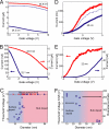
Diameter-dependent transport behavior of n-type Si NWs. (A) Averaged cross-sectional height profiles determined from AFM images before (red) and after (blue) oxidation and etching of a NW. (Inset) the topographical AFM image, the yellow rectangle indicates the ≈500 nm × 1,000 nm averaging area. (B and C) Series of I–Vg curves at Vsd = 1 V measured from NWs after oxidation and etching with different as-grown diameters. I–Vg curves at Vsd = 1V measured from large (D) and small (E) diameter control NWs (red) and NWs after (solid blue) oxidation and etching. The blue dashed line in D is the I–Vg curve calculated from the control NW (red line) after a single oxidation/etching cycle based on a uniform bulk doping model. The diameters labeled in B–E for blue curves are as-grown diameters before the oxidation and etching process; the diameters for red curves correspond to diameter of the control NW. (F) Diameter dependence of threshold voltage. Blue (red) squares represent data from NWs after oxidation and etching (control NWs). The blue (pink) shaded areas highlight diameters of NWs that do (do not) exhibit clear depletion behavior after a single oxidation/etch cycle.
Fig. 3.
Fig. 3.
Diameter-dependent transport behavior of p-type Si and n-type Ge NWs. (A and B) I–Vg curves at Vsd = 1 V measured from as grown p-Si NWs (red) and NWs after a single oxidation/etch cycle (solid blue). (C) Diameter dependence of threshold voltage for p-Si NWs. Blue and red squares represent data from p-Si NWs after oxidation/etch cycle and as-grown NWs, respectively. The blue (pink) shaded areas highlight diameters of NWs that do (do not) exhibit clear depletion behavior after a single oxidation/etch cycle. (D and E) I–Vg curves at Vsd = 1 V for same n-GeNWs before (red) and after (solid blue) etching. Blue dashed lines in A and D are I–Vg curves calculated from the control (red lines) based on the uniform bulk doping model. (F) Diameter dependence of Vth and resistance ratio for n-Ge NWs. The blue (pink) shaded areas highlight diameters of n-Ge NWs that do (do not) exhibit large threshold voltage shift and resistance ratio after removal of a thin surface layer. All diameters labeled in this figure are as-grown diameters.
Fig. 4.
Fig. 4.
Diameter dependent dopant distribution. (A) Comparison of I–Vg curves at Vsd = 1 V between different diameter n-type Si NWs after 4 cycles of oxidation and etching. D (D0) is the diameter after (before) oxidation and etching. (B) Schematic of dopant distribution. Pink and dark pink shaded parts together represent heavily doped regions, with darkness of the pink color indicating the relative dopant concentration (darker = higher), and blue corresponds to intrinsic region.

References

    1. Sze SM. Semiconductor Devices Physics and Technology. New York: Wiley; 2002.
    1. Singh J. Semiconductor Optoelectronics Physics and Technology. New York: McGraw-Hill; 1995.
    1. Erwin SC, et al. Doping semiconductor nanocrystals. Nature. 2005;436:91–94. - PubMed
    1. Dalpian GM, Chelikowsky JR. Self-purification in semiconductor nanocrystals. Phys Rev Lett. 2006;96:226802. - PubMed
    1. Feng X, et al. Converting ceria polyhedral nanoparticles into single-crystal nanospheres. Science. 2006;312:1504–1508. - PubMed

Publication types

LinkOut - more resources