

A method for nanofluidic device prototyping using elastomeric collapse
- PMID: 19717418
- PMCID: PMC2747158
- DOI: 10.1073/pnas.0904004106
A method for nanofluidic device prototyping using elastomeric collapse
Abstract
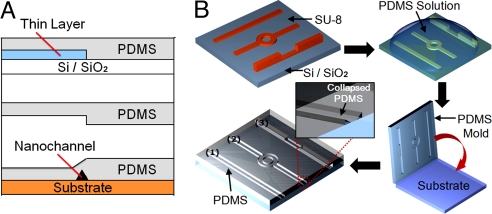
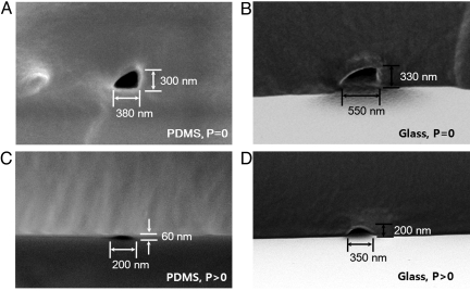
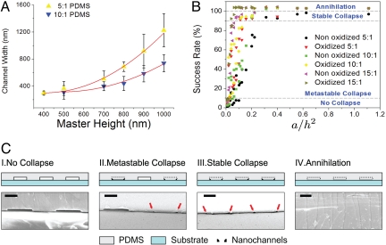
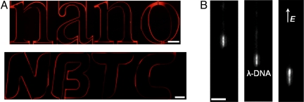
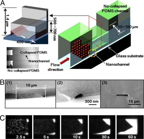
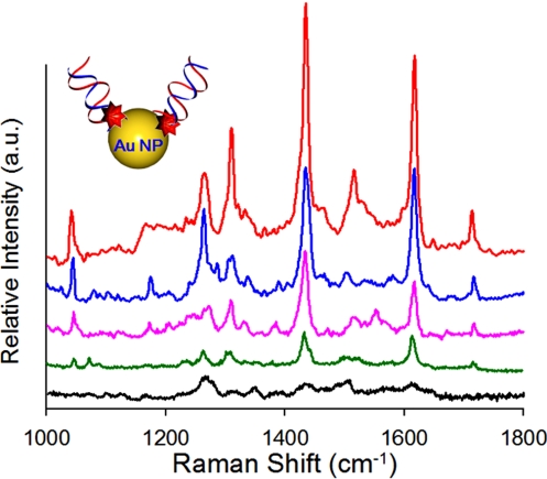
Nanofluidics represents a promising solution to problems in fields ranging from biomolecular analysis to optical property tuning. Recently a number of simple nanofluidic fabrication techniques have been introduced that exploit the deformability of elastomeric materials like polydimethylsiloxane (PDMS). These techniques are limited by the complexity of the devices that can be fabricated, which can only create straight or irregular channels normal to the direction of an applied strain. Here, we report a technique for nanofluidic fabrication based on the controlled collapse of microchannel structures. As is demonstrated, this method converts the easy to control vertical dimension of a PDMS mold to the lateral dimension of a nanochannel. We demonstrate here the creation of complex nanochannel structures as small as 60 nm and provide simple design rules for determining the conditions under which nanochannel formation will occur. The applicability of the technique to biomolecular analysis is demonstrated by showing DNA elongation in a nanochannel and a technique for optofluidic surface enhanced Raman detection of nucleic acids.
Conflict of interest statement
The authors declare no conflict of interest.
Figures
Similar articles
-
DNA manipulation with elastomeric nanostructures fabricated by soft-moulding of a FIB-patterned stamp.Lab Chip. 2011 Aug 7;11(15):2625-9. doi: 10.1039/c1lc20411d. Epub 2011 Jun 15. Lab Chip. 2011. PMID: 21677946
-
A simple polysilsesquioxane sealing of nanofluidic channels below 10 nm at room temperature.Lab Chip. 2007 Sep;7(9):1198-201. doi: 10.1039/b704851c. Epub 2007 Jun 29. Lab Chip. 2007. PMID: 17713620
-
Injection molded nanofluidic chips: fabrication method and functional tests using single-molecule DNA experiments.Lab Chip. 2011 Jan 21;11(2):303-8. doi: 10.1039/c0lc00260g. Epub 2010 Nov 8. Lab Chip. 2011. PMID: 21057689
-
Fabrication of nanofluidic biochips with nanochannels for applications in DNA analysis.Small. 2012 Sep 24;8(18):2787-801. doi: 10.1002/smll.201200240. Epub 2012 Jul 9. Small. 2012. PMID: 22778064 Review.
-
Technologies for nanofluidic systems: top-down vs. bottom-up--a review.Lab Chip. 2005 May;5(5):492-500. doi: 10.1039/b416951d. Epub 2005 Mar 22. Lab Chip. 2005. PMID: 15856084 Review.
Cited by
-
Fabrication of long poly(dimethyl siloxane) nanochannels by replicating protein deposit from confined solution evaporation.Biomicrofluidics. 2012 Jun 19;6(2):26504. doi: 10.1063/1.4730371. Print 2012 Jun. Biomicrofluidics. 2012. PMID: 23781292 Free PMC article.
-
Microfluidic Lab-on-a-Chip for Studies of Cell Migration under Spatial Confinement.Biosensors (Basel). 2022 Aug 5;12(8):604. doi: 10.3390/bios12080604. Biosensors (Basel). 2022. PMID: 36004998 Free PMC article. Review.
-
From cleanroom to desktop: emerging micro-nanofabrication technology for biomedical applications.Ann Biomed Eng. 2011 Feb;39(2):600-20. doi: 10.1007/s10439-010-0218-9. Epub 2010 Dec 14. Ann Biomed Eng. 2011. PMID: 21161384 Free PMC article. Review.
-
A microarray biosensor for multiplexed detection of microbes using grating-coupled surface plasmon resonance imaging.Environ Sci Technol. 2012 Jan 3;46(1):348-59. doi: 10.1021/es201239f. Epub 2011 Dec 1. Environ Sci Technol. 2012. PMID: 22029256 Free PMC article.
-
Fabrication of nanochannels on polystyrene surface.Biomicrofluidics. 2015 Apr 17;9(2):024117. doi: 10.1063/1.4918643. eCollection 2015 Mar. Biomicrofluidics. 2015. PMID: 25945143 Free PMC article.
References
-
- Hong JW, Quake SR. Integrated nanoliter systems. Nat Biotechnol. 2003;21:1179–1183. - PubMed
-
- Han J, Craighead HG. Separation of long DNA molecules in a microfabricated entropic trap array. Science. 2000;288:1026–1029. - PubMed
-
- Austin R. Nanofluidics: A fork in the nano-road. Nat Nanotechnol. 2007;2:79–80. - PubMed
Publication types
MeSH terms
Substances
Grants and funding
LinkOut - more resources
Full Text Sources
Other Literature Sources
Research Materials
