

doi: 10.1002/smll.200901198.
Matrix-assisted dip-pen nanolithography and polymer pen lithography
Affiliations
- PMID: 19885890
- PMCID: PMC3517014
- DOI: 10.1002/smll.200901198
Item in Clipboard
Matrix-assisted dip-pen nanolithography and polymer pen lithography
Small.
.
Abstract
The controlled patterning of nanomaterials presents a major challenge to the field of nanolithography because of differences in size, shape and solubility of these materials. Matrix-assisted dip-pen nanolithography and polymer pen lithography provide a solution to this problem by utilizing a polymeric matrix that encapsulates the nanomaterials and delivers them to surfaces with precise control of feature size.
Figures
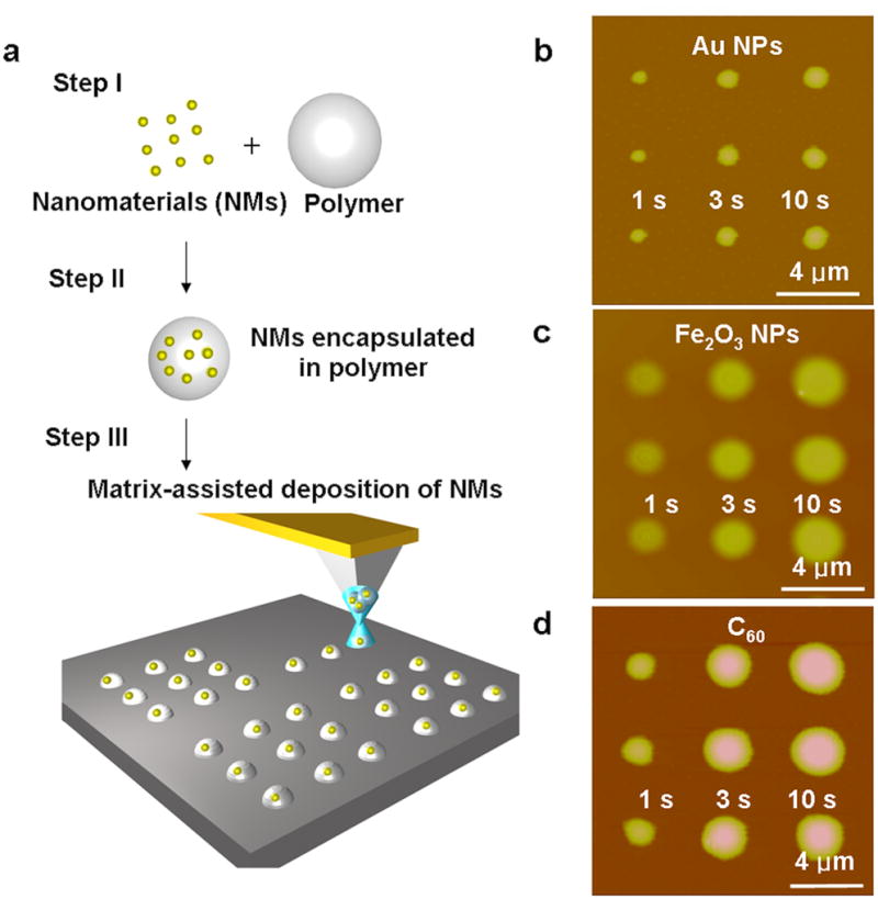
Illustration of matrix-assisted dip-pen nanolithography (MA-DPN) and arrays generated by MA-DPN. a, Scheme illustrating the process involved in patterning surfaces by MA-DPN. b, AFM topographical image of a pattern of three dots of PEG-AuNPs of different sizes on an Au surface created by intentionally varying the dwell time (1, 3 and 10 s) of the tip on the surface. c, AFM topographical image of a pattern of dot arrays of PEG-Fe3O4 MNP dots of different sizes on a Si/SiOx surface created by intentionally varying the dwell time (1, 3 and 10 s) of the tip on the surface. d, AFM topographical image of a pattern of dot arrays of PEG-C60 of different sizes on a Si/SiOx surface created by intentionally varying the dwell time (1, 3 and 10 s) of the tip on the surface.
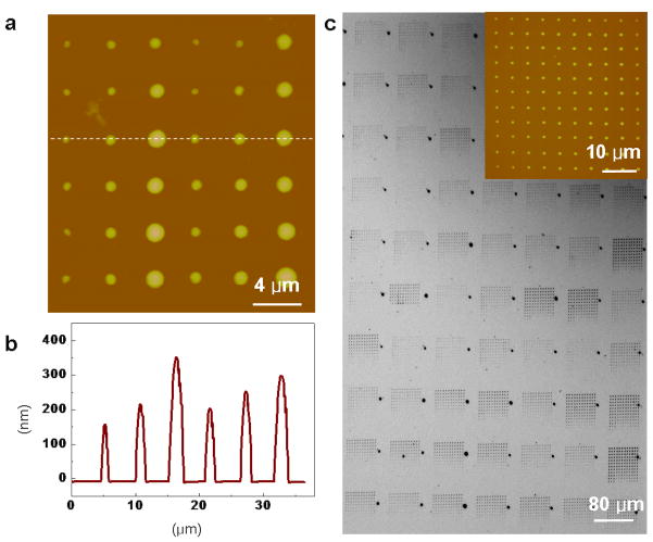
Arrays of dots created by matrix-assisted polymer pen nanolithography (MA-PPL). a, AFM topographical image of a 6×6 dot array of PEG-Fe3O4 MNP ink on a HMDS-coated Si/SiOx surface created by intentionally varying the dwell times of the polymer tips on the surface (1, 3 and 10 s). b, Height profile of one line of PEG-Fe3O4 MNPdots demonstrating control of feature size with varying dwell times. c, An optical microscopy image of a large- scale pattern of PEG-Fe3O4 MNP dots (~1 μm width, 1 s dwell time) created on a HMDS-coated Si/SiOx surface by a 62,500 pen array. The inset is an AFM topographical image of the 12×12 dot pattern of PEG-Fe3O4 ink written by a single polymer pen.
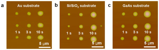
MA-PPL printed dot arrays on metallic, insulating, and semiconducting surfaces. a, A 3×3 dot array of PEG-Fe3O4 MNP ink patterned by MA-PPL on an Au substrate by intentionally varying the dwell time (1, 3 and 10s). b, A 3×3 dot array of PEG-Fe3O4 MNP ink patterned by MA-PPL on a Si/SiOx substrate by varying the dwell time (1, 3 and 10s). c, A 3a3 dot array of PEG-Fe3O4 MNP ink patterned by MA-PPL on a GaAs substrate by intentionally varying the dwell time (1, 3 and 10s).
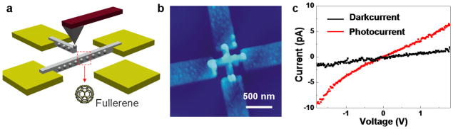
A photoresponsive transistor by MA-DPN. a, Illustration of the deposition of the C60-PEG ink between electrodes by MA-DPN. b, AFM topographical image of the photoresponsive transistor. The four electrodes are connected by two perpendicular lines of the C60-PEG ink. c, The I–V curve of the transistor in the dark (black trace) and under white light from a 50 W tungsten-halogen lamp (red trace).
Similar articles
-
Hard Transparent Arrays for Polymer Pen Lithography.ACS Nano. 2016 Mar 22;10(3):3144-8. doi: 10.1021/acsnano.6b00528. Epub 2016 Mar 1. ACS Nano. 2016. PMID: 26928012 Free PMC article.
-
Tailoring nanostructures using copolymer nanoimprint lithography.Adv Mater. 2012 Apr 17;24(15):1952-5. doi: 10.1002/adma.201103532. Epub 2012 Mar 21. Adv Mater. 2012. PMID: 22434566
-
"Force-feedback" leveling of massively parallel arrays in polymer pen lithography.Nano Lett. 2010 Apr 14;10(4):1335-40. doi: 10.1021/nl904200t. Nano Lett. 2010. PMID: 20184292 Free PMC article.
-
Molecular printing.Nat Chem. 2009 Aug;1(5):353-8. doi: 10.1038/nchem.258. Epub 2009 Jun 28. Nat Chem. 2009. PMID: 21378889 Free PMC article. Review.
-
Patterned polymer brushes.Chem Soc Rev. 2012 Apr 21;41(8):3280-96. doi: 10.1039/c2cs15225h. Epub 2012 Jan 10. Chem Soc Rev. 2012. PMID: 22234473 Review.
Cited by
-
Design of Elastomer-CNT Film Photoactuators for Nanolithography.Polymers (Basel). 2019 Feb 13;11(2):314. doi: 10.3390/polym11020314. Polymers (Basel). 2019. PMID: 30960297 Free PMC article.
-
Beam pen lithography as a new tool for spatially controlled photochemistry, and its utilization in the synthesis of multivalent glycan arrays.Chem Sci. 2014 May 1;5(5):2023-2030. doi: 10.1039/c3sc53315h. Epub 2014 Feb 4. Chem Sci. 2014. PMID: 34113434 Free PMC article.
-
Delineating the pathways for the site-directed synthesis of individual nanoparticles on surfaces.Proc Natl Acad Sci U S A. 2013 Jan 15;110(3):887-91. doi: 10.1073/pnas.1220689110. Epub 2012 Dec 31. Proc Natl Acad Sci U S A. 2013. PMID: 23277538 Free PMC article.
-
Beam pen lithography.Nat Nanotechnol. 2010 Sep;5(9):637-40. doi: 10.1038/nnano.2010.161. Epub 2010 Aug 1. Nat Nanotechnol. 2010. PMID: 20676088
-
Scanning probe block copolymer lithography.Proc Natl Acad Sci U S A. 2010 Nov 23;107(47):20202-6. doi: 10.1073/pnas.1014892107. Epub 2010 Nov 8. Proc Natl Acad Sci U S A. 2010. PMID: 21059942 Free PMC article.
References
-
- Xia YN, Rogers JA, Paul KE, Whitesides GM. Chem Rev. 1999;99:1823. - PubMed
-
- Gates BD, Xu QB, Stewart M, Ryan D, Willson CG, Whitesides GM. Chem Rev. 2005;105:1171. - PubMed
-
- Coskun UC, et al. Appl Phys Lett. 2008;93:123101.
-
- Mendes P, et al. Langmuir. 2004;20:3766. - PubMed
-
- Ko S, et al. Nano Lett. 2007;7:1869. - PubMed
Publication types
MeSH terms
Substances
Grants and funding
LinkOut - more resources
Full Text Sources
Other Literature Sources
