Vertically integrated, three-dimensional nanowire complementary metal-oxide-semiconductor circuits
- PMID: 19940239
- PMCID: PMC2783010
- DOI: 10.1073/pnas.0911713106
Vertically integrated, three-dimensional nanowire complementary metal-oxide-semiconductor circuits
Abstract
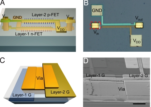
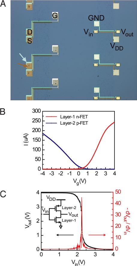
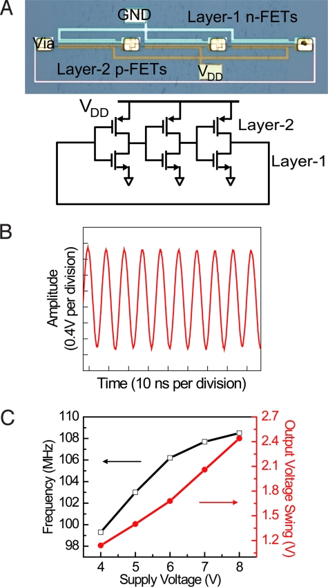
Three-dimensional (3D), multi-transistor-layer, integrated circuits represent an important technological pursuit promising advantages in integration density, operation speed, and power consumption compared with 2D circuits. We report fully functional, 3D integrated complementary metal-oxide-semiconductor (CMOS) circuits based on separate interconnected layers of high-mobility n-type indium arsenide (n-InAs) and p-type germanium/silicon core/shell (p-Ge/Si) nanowire (NW) field-effect transistors (FETs). The DC voltage output (V(out)) versus input (V(in)) response of vertically interconnected CMOS inverters showed sharp switching at close to the ideal value of one-half the supply voltage and, moreover, exhibited substantial DC gain of approximately 45. The gain and the rail-to-rail output switching are consistent with the large noise margin and minimal static power consumption of CMOS. Vertically interconnected, three-stage CMOS ring oscillators were also fabricated by using layer-1 InAs NW n-FETs and layer-2 Ge/Si NW p-FETs. Significantly, measurements of these circuits demonstrated stable, self-sustained oscillations with a maximum frequency of 108 MHz, which represents the highest-frequency integrated circuit based on chemically synthesized nanoscale materials. These results highlight the flexibility of bottom-up assembly of distinct nanoscale materials and suggest substantial promise for 3D integrated circuits.
Conflict of interest statement
The authors declare no conflict of interest.
Figures
References
-
- Topol AW, et al. Three-dimensional integrated circuits. IBM J Res Dev. 2006;50:491–506.
-
- Das S, Chandrakasan A, Reif R. Three-dimensional integrated circuits: Performance, design methodology, and CAD tools. Proc IEEE Comput Soc Annu Symp VLSI. 2003;2003:13–18.
-
- Lieber CM. Nanoscale science and technology: Building a big future from small things. MRS Bull. 2003;28:486–491.
-
- Lieber CM, Wang ZL. Functional nanowires. MRS Bull. 2007;32:99–104.
-
- Thelander C, et al. Nanowire-based one-dimensional electronics. Mater Today. 2006;9:28–35.
LinkOut - more resources
Full Text Sources
Other Literature Sources