Fabrication of a cyclic olefin copolymer planar waveguide embedded in a multi-channel poly(methyl methacrylate) fluidic chip for evanescence excitation
- PMID: 20024052
- PMCID: PMC2859618
- DOI: 10.1039/b908759a
Fabrication of a cyclic olefin copolymer planar waveguide embedded in a multi-channel poly(methyl methacrylate) fluidic chip for evanescence excitation
Abstract
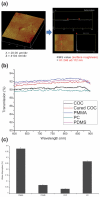
The fabrication and characterization of a novel cyclic olefin copolymer (COC) waveguide embedded in a poly(methyl methacrylate), PMMA, fluidic chip configured in a multi-channel format with an integrated monolithic prism for evanescent fluorescence excitation are reported. The fabrication approach allowed the embedded waveguide to be situated orthogonal to a series of fluidic channels within the PMMA wafer to sample fluorescent solutions in these channels using the evanescence properties of the waveguide. Construction of the device was achieved using several fabrication techniques including high precision micromilling, hot embossing and stenciling of a polymer melt to form the waveguide and coupling prism. A waveguide channel was fabricated in the fluidic chip's cover plate, also made from PMMA, and was loaded with a COC solution using a pre-cast poly(dimethylsiloxane), PDMS, stencil containing a prism-shaped recess. The PMMA substrate contained multiple channels (100 microm wide x 30 microm deep with a pitch of 100 microm) that were situated orthogonal to the waveguide to allow penetration of the evanescent field into the sampling solution. The optical properties of the waveguide in terms of its transmission properties and penetration depth of the evanescent field in the adjacent solution were evaluated. Finally, the device was used for laser-induced fluorescence evanescent excitation of a dye solution hydrodynamically flowing through multiple microfluidic channels in the chip and processed using a microscope equipped with a charge-coupled device (CCD) for parallel readout. The device and optical system were able to image 11 channels simultaneously with a limit-of-detection of 7.1 x 10(-20) mol at a signal-to-noise ratio of 2. The waveguide was simple to manufacture and could be scaled to illuminate much higher channel numbers making it appropriate for high-throughput measurements using evanescent excitation.
Figures


Similar articles
-
An integrated, optofluidic system with aligned optical waveguides, microlenses, and coupling prisms for fluorescence sensing.J Microelectromech Syst. 2020 Aug;29(4):600-609. doi: 10.1109/jmems.2020.3004374. Epub 2020 Jul 2. J Microelectromech Syst. 2020. PMID: 39391841 Free PMC article.
-
Micro-macro hybrid soft-lithography master (MMHSM) fabrication for lab-on-a-chip applications.Biomed Microdevices. 2010 Apr;12(2):345-51. doi: 10.1007/s10544-009-9390-9. Biomed Microdevices. 2010. PMID: 20049640 Free PMC article.
-
Microfluidic devices fabricated in poly(methyl methacrylate) using hot-embossing with integrated sampling capillary and fiber optics for fluorescence detection.Lab Chip. 2002 May;2(2):88-95. doi: 10.1039/b200370h. Epub 2002 Mar 28. Lab Chip. 2002. PMID: 15100840
-
Simple replication methods for producing nanoslits in thermoplastics and the transport dynamics of double-stranded DNA through these slits.Lab Chip. 2010 Dec 7;10(23):3255-64. doi: 10.1039/c0lc00096e. Epub 2010 Oct 11. Lab Chip. 2010. PMID: 20938506
-
PDMS Bonding Technologies for Microfluidic Applications: A Review.Biosensors (Basel). 2021 Aug 23;11(8):292. doi: 10.3390/bios11080292. Biosensors (Basel). 2021. PMID: 34436094 Free PMC article. Review.
Cited by
-
Milling Positive Master for Polydimethylsiloxane Microfluidic Devices: The Microfabrication and Roughness Issues.Micromachines (Basel). 2017 Sep 21;8(10):287. doi: 10.3390/mi8100287. Micromachines (Basel). 2017. PMID: 30400477 Free PMC article.
-
Photonics on a Budget: Low-Cost Polymer Sensors for a Smarter World.Micromachines (Basel). 2025 Jul 15;16(7):813. doi: 10.3390/mi16070813. Micromachines (Basel). 2025. PMID: 40731722 Free PMC article. Review.
-
Micromilling: a method for ultra-rapid prototyping of plastic microfluidic devices.Lab Chip. 2015 Jun 7;15(11):2364-78. doi: 10.1039/c5lc00234f. Lab Chip. 2015. PMID: 25906246 Free PMC article. Review.
-
Rapid fabrication of a microdevice with concave microwells and its application in embryoid body formation.Biomicrofluidics. 2012 Mar;6(1):16504-1650411. doi: 10.1063/1.3687399. Epub 2012 Feb 24. Biomicrofluidics. 2012. PMID: 22662100 Free PMC article.
-
Characterization and Optimization of Isotachophoresis Parameters for Pacific Blue Succinimidyl Ester Dye on a PDMS Microfluidic Chip.Micromachines (Basel). 2020 Oct 22;11(11):951. doi: 10.3390/mi11110951. Micromachines (Basel). 2020. PMID: 33105673 Free PMC article.
References
-
- Reyes DR, Iossifidis D, Auroux PA, Manz A. Anal. Chem. 2002;74:2623–2636. - PubMed
-
- Auroux PA, Iossifidis D, Reyes DR, Manz A. Anal. Chem. 2002;74:2637–2652. - PubMed
-
- Vilkner T, Janasek D, Manz A. Anal. Chem. 2004;76:3373–3385. - PubMed
-
- Whitesides MG. Nature. 2006;442:368–373. - PubMed
-
- Dittrich SP, Tachikawa K, Manz A. Anal. Chem. 2006;78:3887–3907. - PubMed
Publication types
MeSH terms
Substances
Grants and funding
LinkOut - more resources
Full Text Sources
Other Literature Sources
Miscellaneous

