. 2010 Jan 19;107(3):993-8.
doi: 10.1073/pnas.0909482107. Epub 2010 Jan 11.

Self-assembly of microscopic chiplets at a liquid-liquid-solid interface forming a flexible segmented monocrystalline solar cell

Affiliations

Self-assembly of microscopic chiplets at a liquid-liquid-solid interface forming a flexible segmented monocrystalline solar cell

Robert J Knuesel et al. Proc Natl Acad Sci U S A. .

Abstract

This paper introduces a method for self-assembling and electrically connecting small (20-60 micrometer) semiconductor chiplets at predetermined locations on flexible substrates with high speed (62500 chips/45 s), accuracy (0.9 micrometer, 0.14 degrees), and yield (> 98%). The process takes place at the triple interface between silicone oil, water, and a penetrating solder-patterned substrate. The assembly is driven by a stepwise reduction of interfacial free energy where chips are first collected and preoriented at an oil-water interface before they assemble on a solder-patterned substrate that is pulled through the interface. Patterned transfer occurs in a progressing linear front as the liquid layers recede. The process eliminates the dependency on gravity and sedimentation of prior methods, thereby extending the minimal chip size to the sub-100 micrometer scale. It provides a new route for the field of printable electronics to enable the integration of microscopic high performance inorganic semiconductors on foreign substrates with the freedom to choose target location, pitch, and integration density. As an example we demonstrate a fault-tolerant segmented flexible monocrystalline silicon solar cell, reducing the amount of Si that is used when compared to conventional rigid cells.


Conflict of interest statement

The authors declare no conflict of interest.

Figures

Fig. 1.
Fig. 1.
Procedure of surface tension-directed self-assembly at a liquid–liquid–solid interface employing an energy cascade to (i) move components from a suspension to the interface (55 mJ/m2), (ii) preorient the components within the interface to face in the right direction (90 mJ/m2), and (iii) assemble the components on molten solder through dipping (400 mJ/m2). The illustration depicts the situation for an oil–water interface and chiplets made out of Si (SU-8 is detailed in main body), which carry an Au contact on one face. Depicted Au and Si surfaces are treated using hydrophilic MUA and hydrophobic GPTMS functional groups and yield the tabulated measured contact angles, calculated solid–liquid interfacial energies, and energy differences (gray boxes to the right) required to drive the assembly. The available area and curved shape of the interface cause the components to form a closely packed 2D sheet. Upward motion of substrate yields a dynamic contact angle where the receding water layer becomes sufficiently thin for the gold to contact the solder. Patterned assembly on solder is favored by 400 mJ/m2 within this layer.
Fig. 2.
Fig. 2.
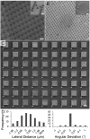
SEM of (A) SU-8 (20 μm side length) and (B, C) Si chiplets (20 μm and 60 μm side length) assembling in regular arrays and arbitrary text patterns (insets). The overlaid CAD guides visible in (C, white lines) are used to measure variations in the center-to-center distance and angular-orientation. (D) Histogram of measured variations. 40 μm scale bars.
Fig. 3.
Fig. 3.
Scaling limits illustrating components and assembly spanning 3 orders of magnitude in size including (A) 1 cm Si cubes (assembly not possible), (B) 1 mm Si blocks (assembly possible), (C) 100 μm Si triangle (assembly possible), and (D) 3 μm-sized SU-8 blocks and discs (discussed in the text).
Fig. 4.
Fig. 4.
Flexible segmented monocrystalline solar cell fabrication procedure, result, and characterization. (A) Assembly and isolation process next to SEM representative of each step. (B) Defect tolerant design strategy and result (SEM) where vacancies are covered with SU-8, preventing shorts to the substrate. (C) Top contact deposition process and representative SEM. (D) Micrograph of an assembled array. (E) IV load curves of cells before (left) and after assembly in unbent (red curve, center) and bent configuration (1 cm radius of curvature, black curve, center); (E, right) IV load curve of a module as depicted in (F); (G) Finite element computer simulation (CoventorWare) of the strain inside the composite flexed (1 cm radius of curvature) structure composed of a 175 μm PET layer holding a 20 μm thin film of Si cubes surrounded by SU-8 where the region of maximum strain is located at the top metal contact between silicon cells and at the chiplet edges. Perspective and side slice views are shown. 60 μm scale bars.

References

    1. Loo Y-L, Willett R, Baldwin K, Rogers J. Additive, nanoscale patterning of metal films with a stamp and a surface chemistry mediated transfer process: Applications in plastic electronics. Appl Phys Lett. 2002;81:562–564.
    1. Ko HC, et al. A hemispherical electronic eye camera based on compressible silicon optoelectronics. Nature. 2008;454:748–753. - PubMed
    1. Kim D-H, et al. Complementary logic gates and ring oscillators on plastic substrates by use of printed ribbons of single-crystalline silicon. IEEE Electron Device L. 2008;29:73–76.
    1. Yoon J, et al. Ultrathin silicon solar microcells for semitransparent, mechanically flexible and microconcentrator module designs. Nat Mater. 2008;7:907–915. - PubMed
    1. Stauth S, Parviz B. Self-assembled single-crystal silicon circuits on plastic. Proc Natl Acad Sci USA. 2006;103:13922–13927. - PMC - PubMed

Publication types