. 2010 Feb 2;107(5):1882-7.
doi: 10.1073/pnas.0914737107. Epub 2010 Jan 19.

Nanowire transistor arrays for mapping neural circuits in acute brain slices

Affiliations

Nanowire transistor arrays for mapping neural circuits in acute brain slices

Quan Qing et al. Proc Natl Acad Sci U S A. .

Abstract

Revealing the functional connectivity in natural neuronal networks is central to understanding circuits in the brain. Here, we show that silicon nanowire field-effect transistor (Si NWFET) arrays fabricated on transparent substrates can be reliably interfaced to acute brain slices. NWFET arrays were readily designed to record across a wide range of length scales, while the transparent device chips enabled imaging of individual cell bodies and identification of areas of healthy neurons at both upper and lower tissue surfaces. Simultaneous NWFET and patch clamp studies enabled unambiguous identification of action potential signals, with additional features detected at earlier times by the nanodevices. NWFET recording at different positions in the absence and presence of synaptic and ion-channel blockers enabled assignment of these features to presynaptic firing and postsynaptic depolarization from regions either close to somata or abundant in dendritic projections. In all cases, the NWFET signal amplitudes were from 0.3-3 mV. In contrast to conventional multielectrode array measurements, the small active surface of the NWFET devices, approximately 0.06 microm(2), provides highly localized multiplexed measurements of neuronal activities with demonstrated sub-millisecond temporal resolution and, significantly, better than 30 microm spatial resolution. In addition, multiplexed mapping with 2D NWFET arrays revealed spatially heterogeneous functional connectivity in the olfactory cortex with a resolution surpassing substantially previous electrical recording techniques. Our demonstration of simultaneous high temporal and spatial resolution recording, as well as mapping of functional connectivity, suggest that NWFETs can become a powerful platform for studying neural circuits in the brain.


Conflict of interest statement

The authors declare no conflict of interest.

Figures

Fig. 1.
Fig. 1.
(A) Measurement schematics. (Top) Overview of a NWFET array fabricated on a transparent substrate with slice oriented with pyramidal cell layer over the devices. (Bottom Left) Zoom-in of device region illustrating interconnected neurons and NWFETs. (Bottom Right) Photograph of the assembled sample chamber. 1, 2, and 3 indicate the mitral cells in the olfactory bulb, the lateral olfactory tract, and the pyramidal cells, resp. 4 and 5 mark the stimulation electrode and the patch clamp pipette, resp. (B) Top view of the NWFET array/brain slice region in fully assembled chamber with medium. Red Box shows a higher resolution image of a single device in contact with the neurons at the bottom of the slice. Blue Box shows the outermost neurons of the slice through an immersed lens from the top. Scale bars are 20 μm. (C) Laminar organization and input circuitry of the piriform cortex (Layer I–III). (D) Conductance recording from a NWFET (Lower Traces) in the same region as neuron used to record cell-attached patch clamp results (Upper Traces). Stimulation in the LOT was performed with strong (200 μA, Red Traces) and weak (50 μA, Blue Traces) 200 μs current pulses. The Open Triangle marks the stimulation pulse.
Fig. 2.
Fig. 2.
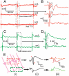
Characteristics and identification of NWFET signals. (A) Conductance vs. time traces from NWFET devices, where each trace has three stimulation events. The Top, Middle, and Bottom Curves correspond to data recorded initially, after the addition of CNQX and APV and after the addition of TTX, resp. Traces are average of three consecutive recordings (n = 3). (B) Expansion of region indicated by Dashed Frame of (A) The Open Triangle and Dashed Oval mark the stimulation and presynaptic features, resp. The Plus and Asterisk mark the postsynaptic features. (C) NWFET conductance vs. time trace recorded in a different position. The Top and Bottom Curves correspond to data recorded initially and after the addition of CNQX and APV, resp. (D) Zoom-in for region indicated by the Dashed Frame in (C). (E) Model explaining different recorded signals. From left to right: (i) Detection region overlapping with cell bodies (Red Frame) or dendrites (Green Frame); (ii) extracellular potential following stimulation exhibits opposite polarities (p-spike is marked by *, and the EPSP is marked by +) in these regions; and (iii) corresponding conductance change of p-type Si NWFET.
Fig. 3.
Fig. 3.
Measurement of signal propagation in LOT with 1D device array. (A) Optical image of the brain slice covering the 1D NWFET array. The 1D array is aligned perpendicularly to the LOT fiber. The Red Circles mark the positions of Devices 1–3 used for recording. The stimulation electrode is positioned at spot one (Red Cross), which is ca. 400 μm away from the array and spot two (Green Cross), which is ca. 1200 μm on the other side. The image is a composite of recorded micrographs. The Dash Line marks the border of the original pictures. The scale bar is 100 μm. Inset is a schematic of experimental configuration. (B) NWFET conductance traces from Devices 1–3 when stimulating at spot one (Red) and two (Green). Data are averaged from eight recordings.
Fig. 4.
Fig. 4.
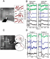
Localized detection with NWFET arrays. (A) (Left) Optical image of brain slice over Si NWFET arrays defined by electron-beam lithography. The Dashed Frames mark the positions of Devices 1–4 and 5 and 6. (Right) Schematics of the devices. (B) Signals obtained from Devices 1–6 with 200 μs stimulation of 2.5 (Left) and 1 mA (Right); n = 21. The Dashed Oval marks the region where signals of opposite polarity were recorded from devices 30 μm apart. (C) (Left) Optical image of brain slice over different design NWFET array. The Dashed Circles mark positions of Devices 1–3 and Device 4. (Right) Schematics of the devices. (D) Signals obtained from Devices 1–4 with stimulation of 1 mA, 200 μs, averaged from n = 11 recordings. The Arrows mark one device picking up a signal; the other 5 μm away does not. The White and Black Scale Bars in (A) and (C) are 100 and 10 μm, resp. The Open Triangles and Filled Triangles in (A) and (C) mark the fine anchor thread used to hold the slice over the device chip and the stimulator, resp. The DC component was removed from traces (1–3 kHz bandpass) shown in (B) and (D).
Fig. 5.
Fig. 5.
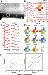
Two-dimensional mapping of heterogeneous activities in the pyramidal cell layer. (A) Optical image of an acute slice over a 4 × 4 NWFET array. Signals were recorded simultaneously from the eight devices indicated on the image. Crosses along the LOT fiber region of the slice mark the stimulation spots A–H. The stimulator insertion depth was not controlled precisely in these experiments. Scale bar represents 100 μm. (B) Signals recorded for devices 1–8 when stimulated with a 200 μs 400 μA pulse. Data are averaged from 15 recordings. The Shaded Area in each trace corresponds to the p-spike and was used to obtain normalized intensity (SI Text Methods). Inset: normalized map of the signal intensity from the 8 Devices. (C) Representative signals recorded from Devices 1 and 8 when stimulating at spots AH with 200 μs and 100 μA pulses. Data are averaged from 12 recordings. (D) Maps of the relative signal intensity or activity for devices 1–8. (E) Correlation between Devices 1 and 8 (Upper Plot) and Devices 3 and 4 (Lower Plot) for the different stimulation positions. The Dashed Black Line marks signals that are correlated. The Dotted Blue Lines mark the uncertainty due to device signal fluctuations determined from correlation analysis (SI Text Methods).

Comment in

  • Nanowire platform for mapping neural circuits.
    Xie C, Cui Y. Xie C, et al. Proc Natl Acad Sci U S A. 2010 Mar 9;107(10):4489-90. doi: 10.1073/pnas.1000450107. Epub 2010 Mar 1. Proc Natl Acad Sci U S A. 2010. PMID: 20194753 Free PMC article. No abstract available.

Similar articles

Cited by

  • Comparative Characterization of NWFET and FinFET Transistor Structures Using TCAD Modeling.
    Petrosyants KO, Silkin DS, Popov DA. Petrosyants KO, et al. Micromachines (Basel). 2022 Aug 11;13(8):1293. doi: 10.3390/mi13081293. Micromachines (Basel). 2022. PMID: 36014213 Free PMC article.
  • Mesh Nanoelectronics: Seamless Integration of Electronics with Tissues.
    Dai X, Hong G, Gao T, Lieber CM. Dai X, et al. Acc Chem Res. 2018 Feb 20;51(2):309-318. doi: 10.1021/acs.accounts.7b00547. Epub 2018 Jan 30. Acc Chem Res. 2018. PMID: 29381054 Free PMC article.
  • Interfacing with the Brain: How Nanotechnology Can Contribute.
    Ahmed AAA, Alegret N, Almeida B, Alvarez-Puebla R, Andrews AM, Ballerini L, Barrios-Capuchino JJ, Becker C, Blick RH, Bonakdar S, Chakraborty I, Chen X, Cheon J, Chilla G, Coelho Conceicao AL, Delehanty J, Dulle M, Efros AL, Epple M, Fedyk M, Feliu N, Feng M, Fernández-Chacón R, Fernandez-Cuesta I, Fertig N, Förster S, Garrido JA, George M, Guse AH, Hampp N, Harberts J, Han J, Heekeren HR, Hofmann UG, Holzapfel M, Hosseinkazemi H, Huang Y, Huber P, Hyeon T, Ingebrandt S, Ienca M, Iske A, Kang Y, Kasieczka G, Kim DH, Kostarelos K, Lee JH, Lin KW, Liu S, Liu X, Liu Y, Lohr C, Mailänder V, Maffongelli L, Megahed S, Mews A, Mutas M, Nack L, Nakatsuka N, Oertner TG, Offenhäusser A, Oheim M, Otange B, Otto F, Patrono E, Peng B, Picchiotti A, Pierini F, Pötter-Nerger M, Pozzi M, Pralle A, Prato M, Qi B, Ramos-Cabrer P, Genger UR, Ritter N, Rittner M, Roy S, Santoro F, Schuck NW, Schulz F, Şeker E, Skiba M, Sosniok M, Stephan H, Wang R, Wang T, Wegner KD, Weiss PS, Xu M, Yang C, Zargarian SS, Zeng Y, Zhou Y, Zhu D, Zierold R, Parak WJ. Ahmed AAA, et al. ACS Nano. 2025 Mar 25;19(11):10630-10717. doi: 10.1021/acsnano.4c10525. Epub 2025 Mar 10. ACS Nano. 2025. PMID: 40063703 Free PMC article. Review.
  • High spatial and temporal resolution wide-field imaging of neuron activity using quantum NV-diamond.
    Hall LT, Beart GC, Thomas EA, Simpson DA, McGuinness LP, Cole JH, Manton JH, Scholten RE, Jelezko F, Wrachtrup J, Petrou S, Hollenberg LC. Hall LT, et al. Sci Rep. 2012;2:401. doi: 10.1038/srep00401. Epub 2012 May 9. Sci Rep. 2012. PMID: 22574249 Free PMC article.
  • Nanowire platform for mapping neural circuits.
    Xie C, Cui Y. Xie C, et al. Proc Natl Acad Sci U S A. 2010 Mar 9;107(10):4489-90. doi: 10.1073/pnas.1000450107. Epub 2010 Mar 1. Proc Natl Acad Sci U S A. 2010. PMID: 20194753 Free PMC article. No abstract available.

References

    1. Shepherd GM. The Synaptic Organization of the Brain. 5th Ed. New York: Oxford Univ Press, Inc.; 2004. Ch. 1, 5, 10, 11.
    1. Taketani M, Baudry M. Advances in Network Electrophysiology Using Multi-Electrode Arrays. New York: Springer Science+Business Media, Inc.; 2006.
    1. Hutzler M, et al. High-resolution multitransistor array recording of electrical field potentials in cultured brain slices. J Neurophysiol. 2006;96:1638–1645. - PubMed
    1. Egert U, Heck D, Aertsen A. Two-dimensional monitoring of spiking networks in acute brain slices. Exp Brain Res. 2002;142:268–274. - PubMed
    1. Wirth C, Lüscher HR. Spatiotemporal evolution of excitation and inhibition in the rat barrel cortex investigated with multielectrode arrays. J Neurophysiol. 2004;91:1635–1647. - PubMed

Publication types

LinkOut - more resources