. 2010 Mar 24;2(24):24ra22.
doi: 10.1126/scitranslmed.3000738.

A conformal, bio-interfaced class of silicon electronics for mapping cardiac electrophysiology

Affiliations

A conformal, bio-interfaced class of silicon electronics for mapping cardiac electrophysiology

Jonathan Viventi et al. Sci Transl Med. .

Abstract

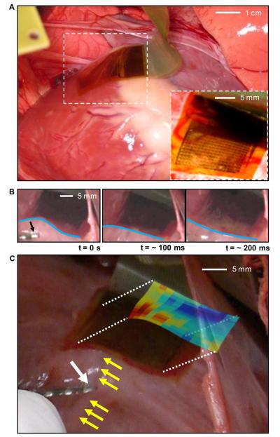
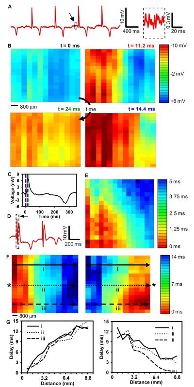
In all current implantable medical devices such as pacemakers, deep brain stimulators, and epilepsy treatment devices, each electrode is independently connected to separate control systems. The ability of these devices to sample and stimulate tissues is hindered by this configuration and by the rigid, planar nature of the electronics and the electrode-tissue interfaces. Here, we report the development of a class of mechanically flexible silicon electronics for multiplexed measurement of signals in an intimate, conformal integrated mode on the dynamic, three-dimensional surfaces of soft tissues in the human body. We demonstrate this technology in sensor systems composed of 2016 silicon nanomembrane transistors configured to record electrical activity directly from the curved, wet surface of a beating porcine heart in vivo. The devices sample with simultaneous submillimeter and submillisecond resolution through 288 amplified and multiplexed channels. We use this system to map the spread of spontaneous and paced ventricular depolarization in real time, at high resolution, on the epicardial surface in a porcine animal model. This demonstration is one example of many possible uses of this technology in minimally invasive medical devices.


Figures

Fig. 1
Fig. 1
Schematic illustration and images corresponding to steps for fabricating active, conformal electronics for cardiac electrophysiology mapping, and photograph of a completed device. (A) Schematic illustration (left) and optical micrograph (right) of a collection of doped silicon nanomembranes in a unit cell. (B) Configuration after fabrication of the source, drain and gate contacts, with suitable interconnects and row electrodes for multiplexed addressing. (C) Configuration after fabrication of the second metal layer, including the column output electrodes. Annotations in the image on the right indicate the multiplexing transistor and the various components of the amplifier. (D) Final layout after deposition of encapsulation layers and fabrication of the contact electrode that provides the interface to the cardiac tissue. (E) Photograph of a completed device, in a slightly bent state. (Inset) A magnified view of a pair of unit cells.
Fig. 2
Fig. 2
Design and electrical properties of an active, flexible device for cardiac electrophysiological mapping. (A) Circuit diagram for a unit cell, with annotations corresponding to those in Fig. 1C. (B) Circuit diagram of four unit cells, indicating the scheme for multiplexed addressing. (C) Current-voltage characteristics of a representative flexible silicon transistor. Drain to source current (Ids) is plotted as a function of drain to source voltages (Vds). The gate to source voltage (Vgs) is varied from 0 to 4V in 1V steps. (Inset) Ids on logarithmic (left) and linear scales (right) as Vgs is swept from −2 to +5V, demonstrating the threshold voltage (Vt) of the transistor. (D) Simulated and measured frequency response of a representative amplifier with multiplexing disabled. The amplifier shows performance properties consistent with design targets and simulations, i.e. −3 db cutoff frequency of ~ 200 kHz. Simulations were obtained using commercial software (Cadence, Cadence Design Systems; see SM for simulation details). (E) Representative multiplexer switching response, showing the row select signals, column output and simulated column output. The response time is limited by the external row select signal slew rate. (F) Percentage of the final voltage value attained during the allotted settling time, averaged across all of the electrodes, for increasing multiplexing frequency, indicating that the maximum useable multiplexing rate is approximately 200 kHz. (G) Photograph of a completed device with ACF interconnect, immersed in a saline solution. (H) Sine wave response (at 10 Hz) before and after saline immersion for 3 hours.
Fig. 3
Fig. 3
Photographs of a flexible EP mapping device in use in a porcine animal model. (A) Photograph of flexible device conforming to the cardiac tissue via surface tension. (Inset) A magnified image at a different viewing angle. (B) Sequence of movie frames collected at different times during the contraction cycle of the heart, illustrating the ability of the device to bend in a way that maintains intimate, conformal contact with the tissue during cardiac rhythm. Blue lines highlight the degree of bending along the device. A conventional pacing electrode is indicated in the left frame (black arrow). (C) Photograph of a device on the left anterior descending (LAD) coronary artery (yellow arrow), with overlaid color map of the relative time of depolarization from paced activation. The white arrow in the lower left indicates the pacing electrode and the red colors in the activation map indicate the areas of earliest response.
Fig. 4
Fig. 4
Representative data recorded from a porcine animal model with a flexible EP mapping device. (A) Representative single voltage trace without external pacing. (Inset) Magnified view of the system noise. Black arrow, source of the inset data. The SNR of the recorded signal was approximately 34 dB. (B) Representative voltage data for all electrodes at four points in time showing normal cardiac wavefront propagation. Voltage is plotted with the color scale in the right corner. (C) Average voltage from all electrodes illustrating the point in time that each frame in (B) was taken (dotted-line). The color of the dashed lines corresponds to the color of the time label in (B). (D) Representative single voltage trace with external pacing from a standard clinical electrode. The black arrow and dotted-line box highlight the pacing artifact. Note that negative is plotted up by convention in A,C, and D. (E) Color map of relative activation times for two different external pacing sites. The activation times are plotted with the color scale shown at the right. Asterisks (*) indicate the relative location of the external pacing electrode. The scale bar illustrates the spacing between electrode locations. The data from the activation map at the locations marked by lines i – iii are plotted in (F). (F) Activation delay plotted as a function of distance from the left side of the array for selected rows indicated by the arrows in (E). Data from 5 columns in B and 6 columns in E were removed due to failures in the metal interconnections.

Similar articles

Cited by

References

    1. Gelinck GH, Huitema HEA, Veenendaal E, Cantatore E, Schrijnemakers L, Putten JBPH, Geuns TCT, Beenhakkers M, Giesbers JB, Huisman B-H, Meijer EJ, Benito EM, Touwslager FJ, Marsman AW, Rens BJE, Leeuw DM. Flexible active-matrix displays and shift registers based on solution-processed organic transistors. Nat. Mater. 2004;3:106–110. - PubMed
    1. Cantatore E, Geuns TCT, Gelinck GH, Veenendaal E, Gruijthuijsen AFA, Schrijnemakers L, Drews S, Leeuw DM. A 13.56-MHz RFID system based on organic transponders. IEEE J. Solid-St. Circ. 2007;42:84–92.
    1. Baca AJ, Ahn J-H, Sun Y, Meitl MA, Menard E, Kim H-S, Choi WM, Kim D-H, Huang Y, Rogers JA. Semiconductor wires and ribbons for high-performance flexible electronics. Angew. Chem. Int. Ed. 2008;47:5524–5542. - PubMed
    1. Khang DY, Jiang H, Huang Y, Rogers JA. A stretchable form of single-crystal silicon for high-performance electronics on rubber substrates. Science. 2006;311:208–212. - PubMed
    1. Kim D-H, Ahn J-H, Choi WM, Kim H-S, Kim T-H, Song J, Huang YY, Liu Z, Lu C, Rogers JA. Stretchable and foldable silicon integrated circuits. Science. 2008;320:507–511. - PubMed

Publication types

LinkOut - more resources