

Top-gated graphene nanoribbon transistors with ultrathin high-k dielectrics
- PMID: 20380441
- PMCID: PMC2965644
- DOI: 10.1021/nl100840z
Top-gated graphene nanoribbon transistors with ultrathin high-k dielectrics
Abstract
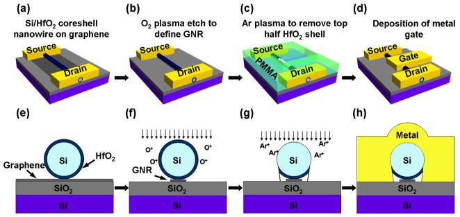
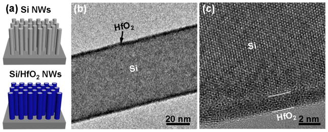
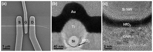
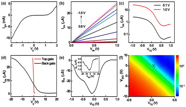
The integration ultrathin high dielectric constant (high-k) materials with graphene nanoribbons (GNRs) for top-gated transistors can push their performance limit for nanoscale electronics. Here we report the assembly of Si/HfO(2) core/shell nanowires on top of individual GNRs as the top-gates for GNR field-effect transistors with ultrathin high-k dielectrics. The Si/HfO(2) core/shell nanowires are synthesized by atomic layer deposition of the HfO(2) shell on highly doped silicon nanowires with a precise control of the dielectric thickness down to 1-2 nm. Using the core/shell nanowires as the top-gates, high-performance GNR transistors have been achieved with transconductance reaching 3.2 mS microm(-1), the highest value for GNR transistors reported to date. This method, for the first time, demonstrates the effective integration of ultrathin high-k dielectrics with graphene with precisely controlled thickness and quality, representing an important step toward high-performance graphene electronics.
Figures
Similar articles
-
High-performance top-gated graphene-nanoribbon transistors using zirconium oxide nanowires as high-dielectric-constant gate dielectrics.Adv Mater. 2010 May 4;22(17):1941-5. doi: 10.1002/adma.200904415. Adv Mater. 2010. PMID: 20526997 Free PMC article. No abstract available.
-
High-kappa oxide nanoribbons as gate dielectrics for high mobility top-gated graphene transistors.Proc Natl Acad Sci U S A. 2010 Apr 13;107(15):6711-5. doi: 10.1073/pnas.0914117107. Epub 2010 Mar 22. Proc Natl Acad Sci U S A. 2010. PMID: 20308584 Free PMC article.
-
Graphene-graphite oxide field-effect transistors.Nano Lett. 2012 Mar 14;12(3):1165-9. doi: 10.1021/nl2028415. Epub 2012 Mar 1. Nano Lett. 2012. PMID: 22380722
-
Graphene-based multilayers constructed from layer-by-layer self-assembly techniques.J Nanosci Nanotechnol. 2014 Feb;14(2):1145-53. doi: 10.1166/jnn.2014.9110. J Nanosci Nanotechnol. 2014. PMID: 24749418 Review.
-
Graphene doping methods and device applications.J Nanosci Nanotechnol. 2014 Feb;14(2):1120-33. doi: 10.1166/jnn.2014.9118. J Nanosci Nanotechnol. 2014. PMID: 24749416 Review.
Cited by
-
Graphene transistors.Nat Nanotechnol. 2010 Jul;5(7):487-96. doi: 10.1038/nnano.2010.89. Epub 2010 May 30. Nat Nanotechnol. 2010. PMID: 20512128
-
Selective nano-buckling improves the performance of graphene logic transistors.Natl Sci Rev. 2024 Jan 3;11(2):nwad316. doi: 10.1093/nsr/nwad316. eCollection 2024 Feb. Natl Sci Rev. 2024. PMID: 38226177 Free PMC article. No abstract available.
-
Sub-100 nm channel length graphene transistors.Nano Lett. 2010 Oct 13;10(10):3952-6. doi: 10.1021/nl101724k. Nano Lett. 2010. PMID: 20815334 Free PMC article.
-
Tunable transport gap in narrow bilayer graphene nanoribbons.Sci Rep. 2013;3:1248. doi: 10.1038/srep01248. Epub 2013 Feb 13. Sci Rep. 2013. PMID: 23409239 Free PMC article.
-
Graphene-Dielectric Integration for Graphene Transistors.Mater Sci Eng R Rep. 2010 Nov 22;70(3-6):354-370. doi: 10.1016/j.mser.2010.07.003. Mater Sci Eng R Rep. 2010. PMID: 21278913 Free PMC article.
References
-
- Novoselov KS, Geim AK, Morozov SV, Jiang D, Zhang Y, Dubonos SV, Grigorieva IV, Firsov AA. Science. 2004;306:666–669. - PubMed
-
- Bunch JS, Yaish Y, Brink M, Bolotin K, McEuen PL. Nano Lett. 2005;5:287–290. - PubMed
-
- Novoselov KS, Geim AK, Morozov SV, Jiang D, Katsnelson MI, Grigorieva IV, Dubonos SV, Firsov AA. Nature. 2005;438:197–200. - PubMed
-
- Zhang YB, Tan YW, Stormer HL, Kim P. Nature. 2005;438:201–204. - PubMed
-
- Berger C, Song ZM, Li XB, Wu XS, Brown N, Naud C, Mayou D, Li TB, Hass J, Marchenkov AN, Conrad EH, First PN, de Heer WA. Science. 2006;312:1191–1196. - PubMed
Publication types
MeSH terms
Substances
Grants and funding
LinkOut - more resources
Full Text Sources
Other Literature Sources
