

Fabricating nanowire devices on diverse substrates by simple transfer-printing methods
- PMID: 20479263
- PMCID: PMC2890492
- DOI: 10.1073/pnas.0914031107
Fabricating nanowire devices on diverse substrates by simple transfer-printing methods
Abstract
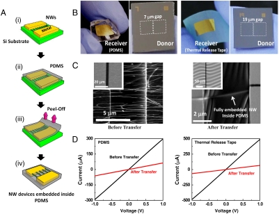
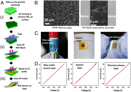
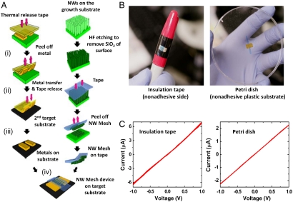
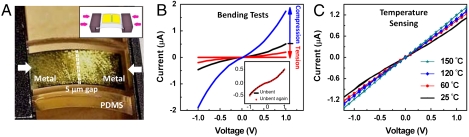
The fabrication of nanowire (NW) devices on diverse substrates is necessary for applications such as flexible electronics, conformable sensors, and transparent solar cells. Although NWs have been fabricated on plastic and glass by lithographic methods, the choice of device substrates is severely limited by the lithographic process temperature and substrate properties. Here we report three new transfer-printing methods for fabricating NW devices on diverse substrates including polydimethylsiloxane, Petri dishes, Kapton tapes, thermal release tapes, and many types of adhesive tapes. These transfer-printing methods rely on the differences in adhesion to transfer NWs, metal films, and devices from weakly adhesive donor substrates to more strongly adhesive receiver substrates. Electrical characterization of fabricated NW devices shows that reliable ohmic contacts are formed between NWs and electrodes. Moreover, we demonstrated that Si NW devices fabricated by the transfer-printing methods are robust piezoresistive stress sensors and temperature sensors with reliable performance.
Conflict of interest statement
The authors declare no conflict of interest.
Figures
Similar articles
-
Fabrication of functional nanowire devices on unconventional substrates using strain-release assembly.ACS Appl Mater Interfaces. 2013 Jan 23;5(2):256-61. doi: 10.1021/am302384z. Epub 2012 Dec 28. ACS Appl Mater Interfaces. 2013. PMID: 23249184
-
Room-temperature compressive transfer printing of nanowires for nanoelectronic devices.Langmuir. 2012 Dec 21;28(51):17851-8. doi: 10.1021/la3036133. Epub 2012 Dec 11. Langmuir. 2012. PMID: 23199260
-
Nanotransplantation Printing of Crystallographic-Orientation-Controlled Single-Crystalline Nanowire Arrays on Diverse Surfaces.ACS Nano. 2017 Nov 28;11(11):11642-11652. doi: 10.1021/acsnano.7b06696. Epub 2017 Nov 13. ACS Nano. 2017. PMID: 29131582
-
Nanowire Assemblies for Flexible Electronic Devices: Recent Advances and Perspectives.Adv Mater. 2018 Nov;30(48):e1803430. doi: 10.1002/adma.201803430. Epub 2018 Oct 25. Adv Mater. 2018. PMID: 30357968 Review.
-
Polymer-Assisted Metal Deposition (PAMD) for Flexible and Wearable Electronics: Principle, Materials, Printing, and Devices.Adv Mater. 2019 Sep;31(37):e1902987. doi: 10.1002/adma.201902987. Epub 2019 Jul 15. Adv Mater. 2019. PMID: 31304644 Review.
Cited by
-
Stretchable ultrasonic transducer arrays for three-dimensional imaging on complex surfaces.Sci Adv. 2018 Mar 23;4(3):eaar3979. doi: 10.1126/sciadv.aar3979. eCollection 2018 Mar. Sci Adv. 2018. PMID: 29740603 Free PMC article.
-
Research Progress of Microtransfer Printing Technology for Flexible Electronic Integrated Manufacturing.Micromachines (Basel). 2021 Nov 3;12(11):1358. doi: 10.3390/mi12111358. Micromachines (Basel). 2021. PMID: 34832770 Free PMC article. Review.
-
Pressure Sensitive Adhesive Tape: A Versatile Material Platform for Optical Sensors.Sensors (Basel). 2020 Sep 16;20(18):5303. doi: 10.3390/s20185303. Sensors (Basel). 2020. PMID: 32948000 Free PMC article. Review.
-
Programmable and scalable transfer printing with high reliability and efficiency for flexible inorganic electronics.Sci Adv. 2020 Jun 17;6(25):eabb2393. doi: 10.1126/sciadv.abb2393. eCollection 2020 Jun. Sci Adv. 2020. PMID: 32596472 Free PMC article.
-
Bio-compatible organic humidity sensor transferred to arbitrary surfaces fabricated using single-cell-thick onion membrane as both the substrate and sensing layer.Sci Rep. 2016 Jul 20;6:30065. doi: 10.1038/srep30065. Sci Rep. 2016. PMID: 27436586 Free PMC article.
References
-
- Lu W, Lieber CM. Semiconductor nanowires. J Phys D Appl Phys. 2006;39(21):R387–R406.
-
- Huang Y, et al. Logic gates and computation from assembled nanowire building blocks. Science. 2001;294(5545):1313–1317. - PubMed
-
- Yan R, et al. Nanowire photonics. Nat Photon. 2009;3(10):569–576.
-
- Zimmler MA, et al. Scalable fabrication of nanowire photonic and electronic circuits using spin-on glass. Nano Lett. 2008;8(6):1695–1699. - PubMed
LinkOut - more resources
Full Text Sources
Other Literature Sources
