. 2010 Jun 8;107(23):10383-8.
doi: 10.1073/pnas.1005892107. Epub 2010 May 24.

Visualizing the formation of the Kondo lattice and the hidden order in URu(2)Si(2)

Affiliations

Visualizing the formation of the Kondo lattice and the hidden order in URu(2)Si(2)

Pegor Aynajian et al. Proc Natl Acad Sci U S A. .

Abstract

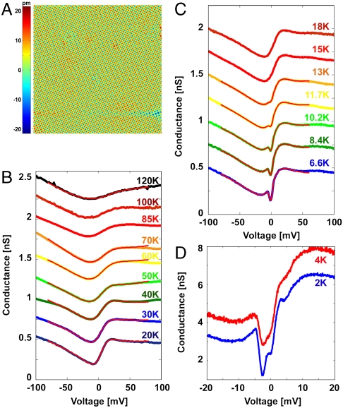
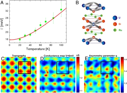
Heavy electronic states originating from the f atomic orbitals underlie a rich variety of quantum phases of matter. We use atomic scale imaging and spectroscopy with the scanning tunneling microscope to examine the novel electronic states that emerge from the uranium f states in URu(2)Si(2). We find that, as the temperature is lowered, partial screening of the f electrons' spins gives rise to a spatially modulated Kondo-Fano resonance that is maximal between the surface U atoms. At T = 17.5 K, URu(2)Si(2) is known to undergo a second-order phase transition from the Kondo lattice state into a phase with a hidden order parameter. From tunneling spectroscopy, we identify a spatially modulated, bias-asymmetric energy gap with a mean-field temperature dependence that develops in the hidden order state. Spectroscopic imaging further reveals a spatial correlation between the hidden order gap and the Kondo resonance, suggesting that the two phenomena involve the same electronic states.


Conflict of interest statement

The authors declare no conflict of interest.

Figures

Fig. 1.
Fig. 1.
STM topography. (A and B) Constant current topographic image (-200 mV, 60 pA, 33 Å) showing an atomically ordered surface (termed surface A) and (100 mV, 200 pA, 90 Å) showing an atomic layer with surface reconstruction (termed surface B), respectively. (C) The relative heights between surfaces A and B. (D) Constant current topographic image (-50 mV, 100 pA) over a 185 × 140 2 area showing a (2 × 1) reconstructed surface (surface C) lying ∼2.2  above surface A. A horizontal line cut through the data in C and D is shown on the bottom panels. (E) Schematic diagram illustrating the different atomic layers of URu2Si2. U is identified as the atomically ordered surface (surface A) that lies 1.24 Å above and 3.56 Å below surface B. In this case, obtaining surfaces A and B requires breaking of a single bond only (U-Si; see arrows). (F) Schematic diagram illustrating a different possibility for the cleaved surfaces, which requires the breaking of two bonds (Ru-Si and U-Si; see arrows). This scenario cannot explain why surfaces A and B occur with roughly equal probabilities. The step heights in A and B are obtained (or calculated) from ref. .
Fig. 2.
Fig. 2.
STM topography and spectroscopy on URu2Si2. (A) Constant current topographic image (-200 mV, 60 pA) over a 200-Å area showing the atomically ordered surface where the spectroscopic measurements are performed. (B and C) Averaged electronic DOS above (B) and below (C) the HO temperature. The red lines in B and C are the results of least squares fit described in the text and SI Text. Spectra are offset by 0.25 nS for clarity. (D) Averaged electronic DOS at low temperatures showing additional features within the gap. Spectra are offset by 1 nS for clarity.
Fig. 3.
Fig. 3.
Kondo lattice. (A) Temperature dependence of the Kondo resonance width Γ extracted from the fits in Fig. 2B. The red line represents the temperature dependence for a single Kondo impurity described in the text, which results in a Kondo temperature TK = 129 ± 10 K. (B) Crystal structure of URu2Si2 indicating the different atomic layers and a schematic of the orbitals that bond the Si atoms to the U atoms. (C) A high-resolution constant current topography of 4 × 4 atoms taken at 18 K. (D) Conductance map at 6 mV (Kondo resonance energy) corresponding to the topography in C showing atomic scale modulations. (E) The dimensionless q(r) map on the same area as in C obtained by fitting the spectra at each location to a Fano line shape. The larger values of q (indicating higher tunneling probability to the Kondo resonance) lie in between the atomic sites as depicted by the black square.
Fig. 4.
Fig. 4.
Temperature dependence of the HO gap. (A and B) The experimental data below THO divided by the 18-K data. The data are fit to the form formula image, which resembles an asymmetric BCS-like DOS with an offset from EF. V0, γ, and formula image 
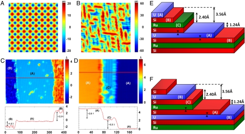
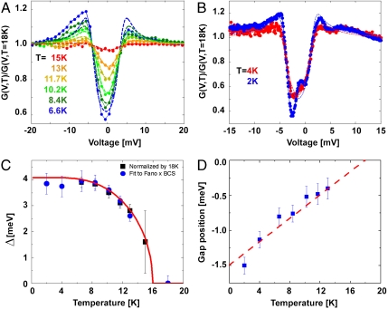
are the gap position (offset from the Fermi energy), the inverse quasi-particle lifetime, and the gap magnitude, respectively. A quasi-particle lifetime broadening of γ ∼ 1.5 mV was extracted from the fits. (C) Temperature dependence of the gap extracted from the fits in A (Black Squares) and from a direct fit to the raw data of Fig. 2C (Blue Circles). Both results are comparable within the error bars. The transition temperature THO = 16.0 ± 0.4 K is slightly lower than the bulk transition temperature presumably as a consequence of the measurement being performed on the surface. (D) Temperature dependence of the gap position Vo extracted from the fits. The line is a guide to the eye.
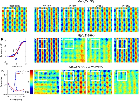
Fig. 5.
Fig. 5.
Atomic origin of the HO. (A) A constant current topography at T = 18 K corresponding to 5 × 5 atoms. Spatial conductance maps on the area in A at different bias voltages V obtained at 18 (BE) and 6.6 K (GJ). The junction is stabilized at -100 mV and 100 pA. All conductance maps are normalized to their mean value to emphasize the atomic contrast. The maps display an atomically periodic modulation. (F) Average dI/dV spectra at 18 and 6.6 K. The arrows indicate the energies where the conductance maps are performed. (LO) Division of the G(r,V,T = 6.6 K) maps with the G(r,V,T = 18 K) maps showing a contrast reversal of the conductance when moving from outside the gap (L; V = -6 mV) to within the gap (M and N). The loss of the spectral weight in the gap and the transfer to higher energies occurs principally between the surface U atoms as is shown by the white square boxes. (K) Correlation of the conductance maps with the atomic locations above and below the HO temperature showing a dramatic change of correlation (change of contrast) within the gapped region between the surface U atoms. Homogeneous gapping should result in no change of correlation.

References

    1. Stewart G. Heavy-fermion systems. Rev Mod Phys. 1984;56(4):755–787.
    1. Fisk Z, Sarrao JL, Smith JL, Thompson JD. The physics and chemistry of heavy fermions. Proc Natl Acad Sci USA. 1995;92:6663–6667. - PMC - PubMed
    1. Mathur ND, et al. Magnetically mediated superconductivity in heavy fermion compounds. Nature. 1998;394:39–43.
    1. Hewson AC. The Kondo Problem to Heavy Fermions. Cambridge, UK: Cambridge Univ Press; 1993.
    1. Coleman P. Handbook of Magnetism and Advanced Magnetic Materials. Vol 1. New York: Wiley; 2007. Heavy Fermions: Electrons at the edge of magnetism.

LinkOut - more resources