

Field Emission of ITO-Coated Vertically Aligned Nanowire Array
- PMID: 20596363
- PMCID: PMC2894224
- DOI: 10.1007/s11671-010-9613-2
Field Emission of ITO-Coated Vertically Aligned Nanowire Array
Abstract
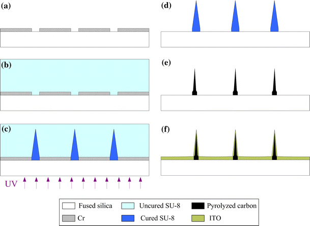
An indium tin oxide (ITO)-coated vertically aligned nanowire array is fabricated, and the field emission characteristics of the nanowire array are investigated. An array of vertically aligned nanowires is considered an ideal structure for a field emitter because of its parallel orientation to the applied electric field. In this letter, a vertically aligned nanowire array is fabricated by modified conventional UV lithography and coated with 0.1-μm-thick ITO. The turn-on electric field intensity is about 2.0 V/μm, and the field enhancement factor, β, is approximately 3,078 when the gap for field emission is 0.6 μm, as measured with a nanomanipulator in a scanning electron microscope.
Keywords: Field emission; ITO; Nanowire; Top–down.
Figures


References
-
- Fowler RH, Nordheim L. Proc. 1928. p. 173. Bibcode number [1928RSPSA.119..173F]
-
- Brodie I, Schwoebel PR. Proc. IEEE. 1994. pp. 1006–1034. COI number [1:CAS:528:DyaK2cXmtFynsLo%3D] - DOI
-
- Milne WI, Teo KBK, Amaratunga GAJ, Lacerda R, Legagneux P, Pirio G, Semet V, Thien Binh V. Curr. 2004. pp. 513–551. - DOI
-
- Wan Q, Feng P, Wang TH. Appl. 2006. p. 123102. Bibcode number [2006ApPhL..89l3102W] - DOI
LinkOut - more resources
Full Text Sources
Miscellaneous
