

doi: 10.1007/s11671-008-9247-9.
Ordered Mesostructured CdS Nanowire Arrays with Rectifying Properties
Affiliations
- PMID: 20596434
- PMCID: PMC2893866
- DOI: 10.1007/s11671-008-9247-9
Item in Clipboard
Ordered Mesostructured CdS Nanowire Arrays with Rectifying Properties
Nanoscale Res Lett.
.
Abstract
Highly ordered mesoporous CdS nanowire arrays were synthesized by using mesoporous silica as hard template and cadmium xanthate (CdR(2)) as a single precursor. Upon etching silica, mesoporous CdS nanowire arrays were produced with a yield as high as 93 wt%. The nanowire arrays were characterized by XRD, N(2) adsorption, TEM, and SEM. The results show that the CdS products replicated from the mesoporous silica SBA-15 hard template possess highly ordered hexagonal mesostructure and fiber-like morphology, analogous to the mother template. The current-voltage characteristics of CdS nanoarrays are strongly nonlinear and asymmetrical, showing rectifying diode-like behavior.
Figures

aSmall-angle diffraction pattern of template-free CdS nanoarrays.bEDS pattern of the template-free CdS nanoarrays.cWAX diffraction curves of CdS nanoarrays present in SBA-15 pore channels and silica-free CdS nanoarrays

aNitrogen sorption isotherms of the samples successively produced in the synthesis: the SBA-15 hard template (■), CdR2@SBA-15 composites (●) prepared by the impregnation of CdR2into SBA-15, CdS@SBA-15 (▲) obtained from the CdR2@SBA-15 calcined at 160 °C, and CdS-SBA-15 replicas (▼) etched by NaOH solution.bThe corresponding pore-size distribution curves ofa

aTEM images of the SBA-15 sample along the direction of the hexagonal pore arrangement.bTEM images of the template-free CdS sample. Insetcanddare corresponding High-magnification TEM images. Inseteis the corresponding SAED pattern ofb
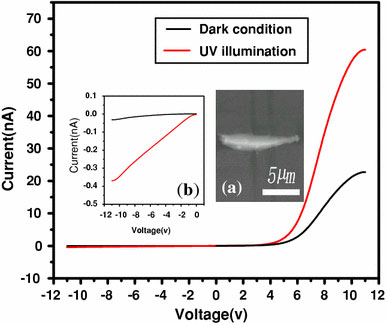
TheI–Vcurves of CdS nanowire arrays at dark and uv-illumination condition. Insetais the SEM image of a bundle of CdS nanowire arrays on Pt electrodes. Insetbis the detailedI–Vcharacteristic of the CdS nanowire arrays under reverse bias

TheI–Vcurves of CdS (a) and ZnS (b) nanoarrays at dark condition
Similar articles
-
Synthesis of highly ordered mesoporous crystalline WS(2) and MoS(2) via a high-temperature reductive sulfuration route.J Am Chem Soc. 2007 Aug 1;129(30):9522-31. doi: 10.1021/ja072910n. Epub 2007 Jul 11. J Am Chem Soc. 2007. PMID: 17625861
-
One-step nanocasting synthesis of highly ordered single crystalline indium oxide nanowire arrays from mesostructured frameworks.J Am Chem Soc. 2003 Apr 23;125(16):4724-5. doi: 10.1021/ja034005i. J Am Chem Soc. 2003. PMID: 12696887
-
High-resolution electron microscopy study of mesoporous dichalcogenides and their hydrogen storage properties.Nanotechnology. 2011 Feb 18;22(7):075702. doi: 10.1088/0957-4484/22/7/075702. Epub 2011 Jan 14. Nanotechnology. 2011. PMID: 21233536
-
Controlled growth of mesostructured crystalline iron oxide nanowires and Fe-filled carbon nanotube arrays templated by mesoporous silica SBA-16 film.J Phys Chem B. 2005 Feb 24;109(7):2546-51. doi: 10.1021/jp0463316. J Phys Chem B. 2005. PMID: 16851255
-
Synthesis of mesoporous carbons using ordered and disordered mesoporous silica templates and polyacrylonitrile as carbon precursor.J Phys Chem B. 2005 May 19;109(19):9216-25. doi: 10.1021/jp045594x. J Phys Chem B. 2005. PMID: 16852101
References
-
- Routkevitch D, Bigioni T, Moskovits M, Xu JM. J. 1996. p. 140. - DOI
LinkOut - more resources
Full Text Sources
