. 2010 Aug 13;329(5993):830-4.
doi: 10.1126/science.1192033.

Three-dimensional, flexible nanoscale field-effect transistors as localized bioprobes

Affiliations

Three-dimensional, flexible nanoscale field-effect transistors as localized bioprobes

Bozhi Tian et al. Science. .

Abstract

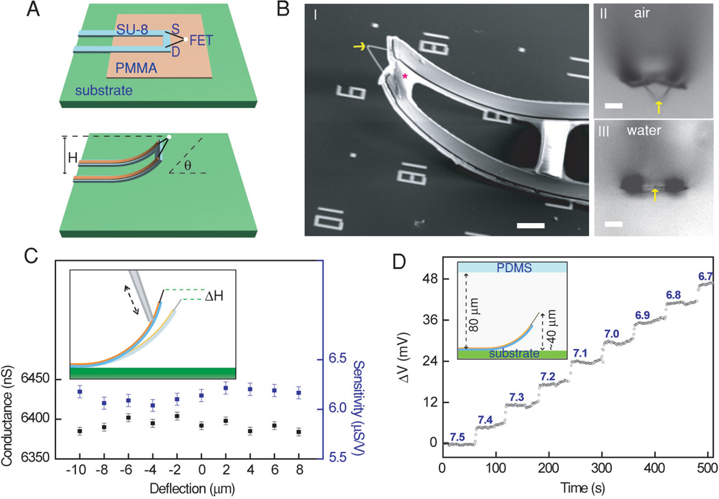
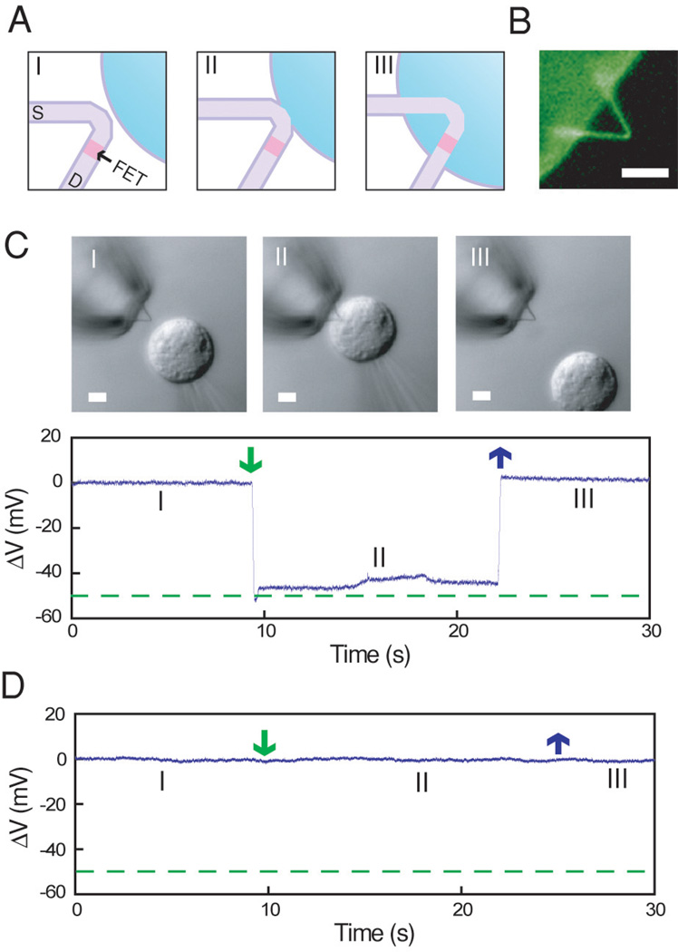
Nanoelectronic devices offer substantial potential for interrogating biological systems, although nearly all work has focused on planar device designs. We have overcome this limitation through synthetic integration of a nanoscale field-effect transistor (nanoFET) device at the tip of an acute-angle kinked silicon nanowire, where nanoscale connections are made by the arms of the kinked nanostructure, and remote multilayer interconnects allow three-dimensional (3D) probe presentation. The acute-angle probe geometry was designed and synthesized by controlling cis versus trans crystal conformations between adjacent kinks, and the nanoFET was localized through modulation doping. 3D nanoFET probes exhibited conductance and sensitivity in aqueous solution, independent of large mechanical deflections, and demonstrated high pH sensitivity. Additionally, 3D nanoprobes modified with phospholipid bilayers can enter single cells to allow robust recording of intracellular potentials.


Figures

Fig. 1
Fig. 1. Synthesis of kinked silicon nanowire probes
A, Schematics of 60° (top) and 0° (middle) multiply-kinked nanowires, and ‘cis’ (top) and ‘trans’ (bottom) configurations in nanowire structures. The blue and magenta regions designate source/drain (S/D) and nanoscale FET channel, respectively. B, SEM image of a doubly-kinked nanowire with ‘cis’ configuration. L is the length of segment between two adjacent kinks. C, cis/(cis + trans) vs. L plot. D, Transmission electron microscopy image of an ultrathin 60° kinked nanowire. Scale bars, 200 nm in B, 50 nm in D.
Fig. 2
Fig. 2. 3D kinked nanowire probes
A, Schematics of device fabrication. Patterned PMMA and SU-8 micro-ribbons [see Materials and Methods (19)] serve as sacrificial layer and flexible device support, respectively. The dimensions of the lightly doped n-type silicon segment (white dots) are ca. 80 × 80 × 200 nm3. H and θ are tip height and orientation, respectively, and “S, D” designate the built-in source and drain connections to the nanoscale FET. B, SEM (I) and bright field optical microscopy (II, III) images of an as-made device. The yellow arrow and magenta star mark the nanoscale FET and SU-8, respectively. II and III are recorded in air and water, respectively. The scale bar is 5 µm. C, Device conductance and sensitivity as a function of deflection of the probe using a micropipette controlled with a micromanipulator. The measurements were carried out in PBS solution. Inset, experimental scheme. D, Change in potential vs. solution pH for a representative 3D nanowire probe. Inset, experimental scheme. For clarity, the ‘point-like’ FET elements are not labelled in schematics in C and D.
Fig. 3
Fig. 3. Surface modification and cellular entry
A, Schematics of nanowire probe entrance into a cell. Purple, light purple, magenta and blue colors denote the phospholipid bilayers, heavily doped nanowire segments, active sensor segment and cytosol, respectively. B, False color fluorescence image of a lipids coated nanowire probe. DMPC was doped with 1 % NBD-dye labelled lipids and imaged through a 510/21 band pass filter. C, Differential interference contrast (DIC) microscopy images (upper panels) and electrical recording (lower panel) of an HL-1 cell and 60° kinked nanowire probe as the cell approaches (I), contacts and internalizes (II), and is retracted from (III) the nanoprobe. A pulled glass micropipette (inner tip diameter, ~ 5 µm) was used to manipulate and voltage-clamp the HL-1 cell. Dashed green line corresponds to the micropipette potential. Scale bars: 5 µm. D, Electrical recording with a 60° kinked nanowire probe without phospholipids surface modification. Green and blue arrows in C and D mark the beginnings of cell penetration and withdrawal, respectively.
Fig. 4
Fig. 4. Electrical recording from beating cardiomyocytes
A, Schematics of cellular recording from cardiomyocyte monolayer on PDMS (left panel), and highlight of extracellular and intracellular nanowire/cell interfaces (middle and right panels). The cell membrane and nanowire lipids coatings are marked as purple lines. B, Electrical recording from beating cardiomyocytes. I) extracellular recording. II) a transition from extracellular to intracellular recordings during cellular entrance and III) steady-state intracellular recording. Green and magenta stars mark the peak positions of intracellular and extracellular signal components, respectively. C, Zoom-in signals from the corresponding red-dashed square regions in (B). Blue and orange stars designate features associated possibly with inward sodium and outward potassium currents, respectively. a-e are five characteristic phases of a cardiac intracellular potential as defined in text. The red-dashed line is the baseline corresponding to intracellular resting state. The cell culture, electronics and recording details are specified in Materials and Methods (19).

Comment in

  • Reading cells from within.
    Pastrana E. Pastrana E. Nat Methods. 2010 Oct;7(10):780-1. doi: 10.1038/nmeth1010-780a. Nat Methods. 2010. PMID: 20936771 No abstract available.

References

    1. Giljohann DA, Mirkin CA. Drivers of biodiagnostic development. Nature. 2009;462:461–464. - PMC - PubMed
    1. Cohen-Karni T, Timko BP, Weiss LE, Lieber CM. Flexible electrical recording from cells using nanowire transistor arrays. Proc. Natl. Acad. Sci. USA. 2009;106:7309–7313. - PMC - PubMed
    1. Eschermann JF, Stockmann R, Hueske M, Vu XT, Ingebrandt S, Offenhausser A. Action potentials of HL-1 cells recorded with silicon nanowire transistors. Appl. Phys. Lett. 2009;95:083703.
    1. Qing Q, Pal SK, Tian BZ, Duan XJ, Timko BP, Cohen-Karni T, Murthy VN, Lieber CM. Nanowire transistor arrays for mapping neural circuits in acute brain slices. Proc. Natl. Acad. Sci. USA. 2010;107:1882–1887. - PMC - PubMed
    1. Heller I, Smaal WTT, Lemay SG, Dekker C. Probing macrophage activity with carbon-nanotube sensors. Small. 2009;5:2528–2532. - PubMed

Publication types