

A Wafer-Scale Etching Technique for High Aspect Ratio Implantable MEMS Structures
- PMID: 20706618
- PMCID: PMC2917827
- DOI: 10.1016/j.sna.2010.06.011
A Wafer-Scale Etching Technique for High Aspect Ratio Implantable MEMS Structures
Abstract
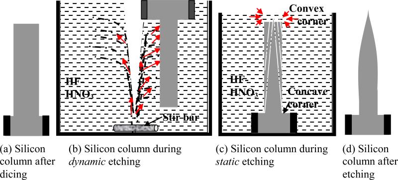
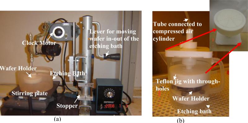
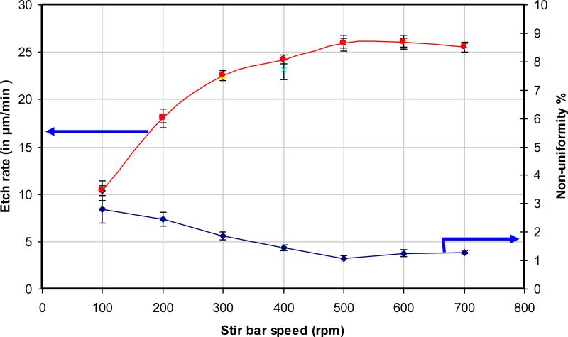
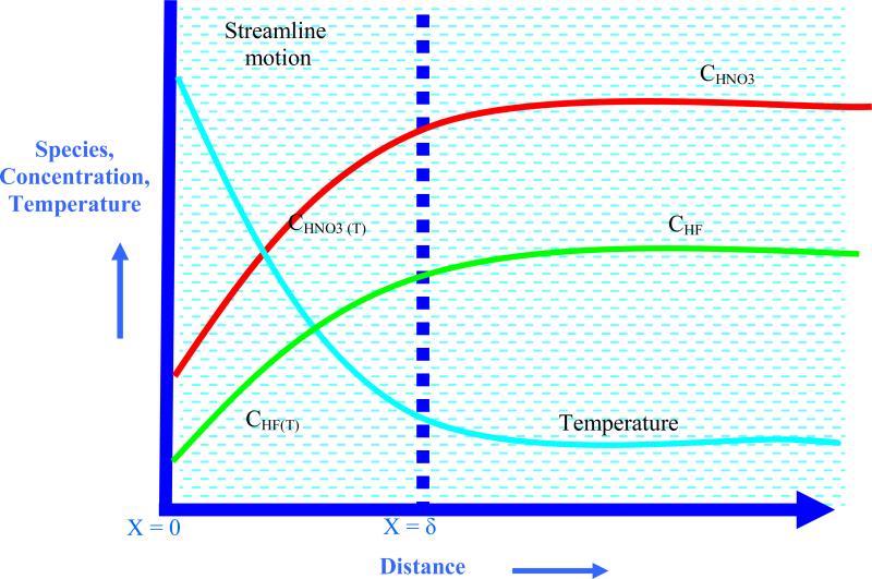
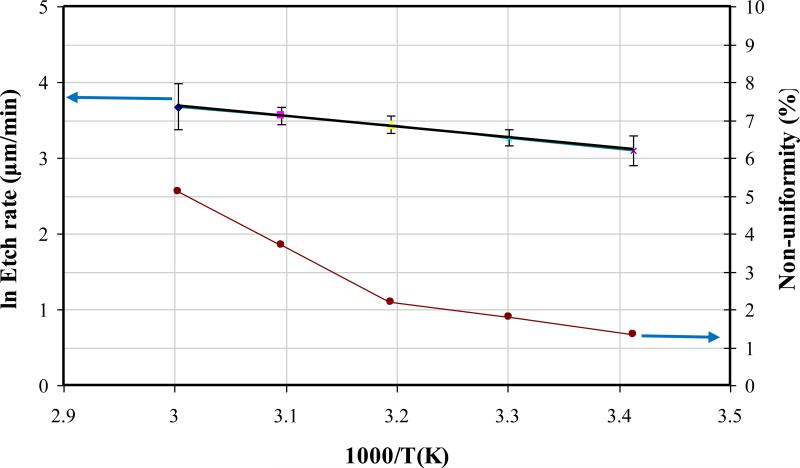
Microsystem technology is well suited to batch fabricate microelectrode arrays, such as the Utah electrode array (UEA), intended for recording and stimulating neural tissue. Fabrication of the UEA is primarily based on the use of dicing and wet etching to achieve high aspect ratio (15:1) penetrating electrodes. An important step in the array fabrication is the etching of electrodes to produce needle-shape electrodes with sharp tips. Traditional etching processes are performed on a single array, and the etching conditions are not optimized. As a result, the process leads to variable geometries of electrodes within an array. Furthermore, the process is not only time consuming but also labor-intensive. This report presents a wafer-scale etching method for the UEA. The method offers several advantages, such as substantial reduction in the processing time, higher throughput and lower cost. More importantly, the method increases the geometrical uniformity from electrode to electrode within an array (1.5 ± 0.5 % non-uniformity), and from array to array within a wafer (2 ± 0.3 % non-uniformity). Also, the etching rate of silicon columns, produced by dicing, are studied as a function of temperature, etching time and stirring rate in a nitric acid rich HF-HNO(3) solution. These parameters were found to be related to the etching rates over the ranges studied and more-importantly affect the uniformity of the etched silicon columns. An optimum etching condition was established to achieve uniform shape electrode arrays on wafer-scale.
Figures
References
-
- Akin T, Najafi K, Smoke RH, Bradley RM. A micromachined silicon sieve electrode for nerve regeneration applications. IEEE Trans.Biomed, Eng. 1994;41:305–313. - PubMed
-
- Edel DJ. A peripheral nerve information transducer for amputees: long-term multichannel recording from rabbit peripheral nerves. IEEE Trans.Biomed, Eng. 1986;33:203–214. - PubMed
-
- BeMent SL, Wise KD, Anderson DJ, Najafi K, Drake KL. Solid-state electrodes for multichannel multiplexed intracortical neuronal recording. IEEE Trans. Biomed, Eng. 1986;33:230–241. - PubMed
-
- Blum NA, Carkhuff BG, Charles HK, Jr., Edwards RL, Meyer RA. Multisite microprobes for neural recording. IEEE Trans. Biomed. Eng. 1991;38:68–74. - PubMed
-
- Drake KL, Wise KD, Farraye J, Anderson DJ, BeMent SL. Performance of planar multisite microprobes in recording extracellular single – unit intracortical activity. IEEE Trans. Biomed, Engg. 1988;35:719–732. - PubMed
Grants and funding
LinkOut - more resources
Full Text Sources
Research Materials
Miscellaneous