. 2010 Sep 16;467(7313):305-8.
doi: 10.1038/nature09405. Epub 2010 Sep 1.

High-speed graphene transistors with a self-aligned nanowire gate

Affiliations

High-speed graphene transistors with a self-aligned nanowire gate

Lei Liao et al. Nature. .

Abstract

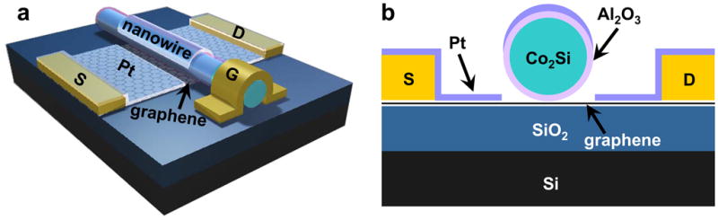
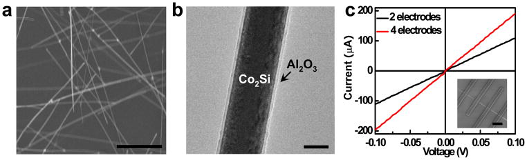
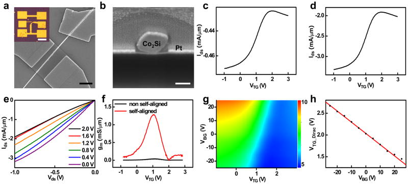
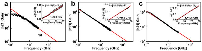
Graphene has attracted considerable interest as a potential new electronic material. With its high carrier mobility, graphene is of particular interest for ultrahigh-speed radio-frequency electronics. However, conventional device fabrication processes cannot readily be applied to produce high-speed graphene transistors because they often introduce significant defects into the monolayer of carbon lattices and severely degrade the device performance. Here we report an approach to the fabrication of high-speed graphene transistors with a self-aligned nanowire gate to prevent such degradation. A Co(2)Si-Al(2)O(3) core-shell nanowire is used as the gate, with the source and drain electrodes defined through a self-alignment process and the channel length defined by the nanowire diameter. The physical assembly of the nanowire gate preserves the high carrier mobility in graphene, and the self-alignment process ensures that the edges of the source, drain and gate electrodes are automatically and precisely positioned so that no overlapping or significant gaps exist between these electrodes, thus minimizing access resistance. It therefore allows for transistor performance not previously possible. Graphene transistors with a channel length as low as 140 nm have been fabricated with the highest scaled on-current (3.32 mA μm(-1)) and transconductance (1.27 mS μm(-1)) reported so far. Significantly, on-chip microwave measurements demonstrate that the self-aligned devices have a high intrinsic cut-off (transit) frequency of f(T) = 100-300 GHz, with the extrinsic f(T) (in the range of a few gigahertz) largely limited by parasitic pad capacitance. The reported intrinsic f(T) of the graphene transistors is comparable to that of the very best high-electron-mobility transistors with similar gate lengths.


Conflict of interest statement

Author Information The authors declare no competing financial interests.

Figures

Figure 1
Figure 1. Schematic illustration of a high-speed graphene transistor with a Co2Si/Al2O3 core/shell nanowire as the self-aligned top-gate
a, Schematic illustration of the three-dimensional view of the device layout. b, Schematic illustration of the cross-sectional view of the device. In this device, the Co2Si/Al2O3 core/shell nanowire defines the channel length, with the 5 nm Al2O3 shell in functioning as the gate dielectrics, and the metallic Co2Si core functioning as the self-integrated local gate, and the self-aligned Pt thin film pads as the source and drain electrodes
Figure 2
Figure 2. Characterization of Co2Si and Co2Si/Al2O3 core/shell nanowires
a, SEM image of the Co2Si nanowires. The nanowires were synthesized through a chemical vapour deposition process with the diameters typically in the range of 100–300 nm and the lengths around 10 μm. b, TEM image of a Co2Si/Al2O3 core/shell nanowire shows a uniform coating of the amorphous Al2O3 (light contrast) surrounding the single-crystal Co2Si core (dark contrast). c, The I–V characteristic of a single Co2Si nanowire in two- and four-terminal measurements to determine the nanowire resistance and resistivity. The inset shows an SEM image of the device, the scale bar is 3 μm.
Figure 3
Figure 3. Room temperature electrical characteristics of the graphene transistors with a self-aligned nanowire gate
a, An SEM images of a graphene transistor with a self-aligned nanowire gate, the width of devices of about 2.64 μm. The inset shows an optical microscope image the overall device layout. b, The cross-sectional SEM image of a typical device shows the self-aligned Pt thin film source and drain electrodes are well separated by the nanowire gate and precisely positioned next to the nanowire gate. The graphene below the nanowire gate is not clearly visible. c, and d, Ids-VTG transfer characteristics at Vds = −1 V before and after the deposition of the self-aligned Pt source-drain electrodes. e, The Ids-Vds output characteristics at various gate voltages (VTG =0.0, 0.4, 0.8, 1.2, 1.6, and 2.0 V) for the dIds self-aligned device. f, Transconductance gm=|dIdsdVg| at Vds = −1 V as a function of top-gate voltage VTG before (black) and after (red) the deposition of the self-aligned Pt source-drain electrodes, highlighting the self-alignment process increases the peak transconductance by a factor of > 60. g, Two dimensional plot of the device conductance for varying VBG and VTG bias for self aligned device. The unit in the color scale is mS. h, The top-gate Dirac point VTG_Dirac at different VBG, with which we can derive CTG/CBG≈38.
Figure 4
Figure 4. Measured small-signal current gain |h21| as a function of frequency f at Vds = −1 V
a, For a device with gate length = 144 nm at VTG = 1 V; b, For a device with gate length = 182 nm at VTG = 0.3 V; and c, For a device with gate length = 210 nm at VTG = 1.1 V; These different VTG values used are the peak transconductance points for each device. The insets show the fT extraction by Gummel’s method.

References

    1. Novoselov KS, et al. Electric field effect in atomically thin carbon films. Science. 2004;306:666–669. - PubMed
    1. Novoselov KS, et al. Two-dimensional gas of massless Dirac fermions in graphene. Nature. 2005;438:197–200. - PubMed
    1. Zhang YB, Tan YW, Stormer HL, Kim P. Experimental observation of the quantum Hall effect and Berry’s phase in graphene. Nature. 2005;438:201–204. - PubMed
    1. Bunch JS, Yaish Y, Brink M, Bolotin K, McEuen PL. Coulomb oscillations and Hall effect in quasi-2D graphite quantum dots. Nano Letters. 2005;5:287–290. - PubMed
    1. Berger C, et al. Electronic confinement and coherence in patterned epitaxial graphene. Science. 2006;312:1191–1196. - PubMed

Publication types