

doi: 10.1021/nl103739n.
Epub 2011 Jan 5.
Smooth growth of organic semiconductor films on graphene for high-efficiency electronics
Affiliations
- PMID: 21207968
- PMCID: PMC3036005
- DOI: 10.1021/nl103739n
Item in Clipboard
Smooth growth of organic semiconductor films on graphene for high-efficiency electronics
Nano Lett.
.
Free PMC article
Abstract
High-quality thin films of conjugated molecules with smooth interfaces are important to assist the advent of organic electronics. Here, we report on the layer-by-layer growth of the organic semiconductor molecule p-sexiphenyl (6P) on the transparent electrode material graphene. Low energy electron microscopy and micro low energy electron diffraction reveal the morphological and structural evolution of the thin film. The layer-by-layer growth of 6P on graphene proceeds by subsequent adding of {111} layers.
Figures
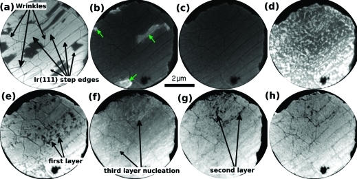
6P layer-by-layer growth on graphene. Sequence of LEEM images taken during the growth of the first three monolayers of 6P on graphene. The field of view (FOV) is 6 μm in all images. (a, t = 134 s) Graphene flake with Ir steps and wrinkles. Steps appear as narrow undulated lines, whereas the straight wrinkles appear as wider lines rotated by 60° with respect to each other. Dark areas are islands that have nucleated next to the wrinkles. (b, t = 1514 s) The islands visible in (a) have formed a closed initial layer (medium gray, marked by arrows). From 400 s onward a second, darker contrast develops on top of the initial layer. This full first monolayer (dark gray) is nearly completed. (c, t = 1698 s) The first monolayer is now completed. The wrinkles are still visible. (d, t = 2107 s) Nucleation of the second layer (bright areas) is observed simultaneously in random positions on the graphene flake. (e, t = 2901 s) The second layer is nearly closed. (f, t = 3467 s) The cycle repeats with the formation of the third layer (bright areas). (g, t = 4429 s) The third layer is nearly closed. (h, t = 5723 s) Another cycle, corresponding to the growth of the fourth layer, starts. The dark spot in the lower part of all images is a defect in the micro channel plate of the LEEM. All images have been adjusted for optimum contrast.
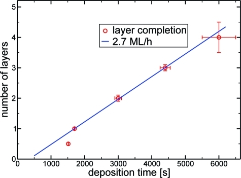
Layer completion times. All but the first data point correspond to the closing of a full monolayer of 6P. From the linear fit (ignoring the first data point) a growth rate of 2.7 ML/h is obtained.
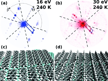
Submonolayer and monolayer structure. (a) μLEED pattern obtained from the first half and (b) the completed first layer. Dashed lines indicate the [1000] (zigzag) direction of the graphene flake. The angles β and Θ used for the description of the unit cells are indicated. Panels (c) and (d) show the proposed structure of the first half and full first layer. (In (c) and (d) planar molecules are used for clarity.)
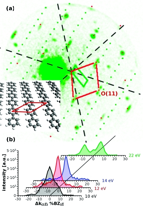
μLEED pattern obtained from a 4.5 ML thick 6P film on graphene. (a) The measured unit cell parameters for the green cell are a = 26.9 Å, b = 9.2 Å, with β = 74° and Θ = 77°. The red unit cell with a size of a = 6.8 Å, b = 6.4 Å, with β = 75° and Θ = 141°, results from diffraction of the individual phenyl rings. The inset shows the real space structure of the adlayer together with the unit cell (solid red line). (b) Spot profiles of the O(11)-spot belonging to the red unit cell in panel (a) . The profiles for different electron energies have been shifted to enhance visibility.
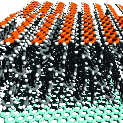
Proposed structure of 6P on metal supported graphene. Four Layers of bulklike 6P are deposited with their {11̅1̅} plane parallel to the graphene substrate (light blue carbon atoms for clarity). The adlayer covering 50% of the top surface is shown with orange carbon atoms.
Similar articles
-
Clean graphene electrodes on organic thin-film devices via orthogonal fluorinated chemistry.Nano Lett. 2015 Apr 8;15(4):2555-61. doi: 10.1021/acs.nanolett.5b00110. Epub 2015 Mar 23. Nano Lett. 2015. PMID: 25774924
-
Transfer of large-area graphene films for high-performance transparent conductive electrodes.Nano Lett. 2009 Dec;9(12):4359-63. doi: 10.1021/nl902623y. Nano Lett. 2009. PMID: 19845330
-
Mesoporous silica nanolayers infiltrated with hole-transporting molecules for hybrid organic light-emitting devices.ACS Nano. 2008 Jun;2(6):1137-42. doi: 10.1021/nn7003124. ACS Nano. 2008. PMID: 19206331
-
Graphene synthesis: relationship to applications.Nanoscale. 2013 Jan 7;5(1):38-51. doi: 10.1039/c2nr32629a. Epub 2012 Nov 19. Nanoscale. 2013. PMID: 23160190 Review.
-
Synthesis of graphene-conjugated polymer nanocomposites for electronic device applications.Nanoscale. 2013 Feb 21;5(4):1440-51. doi: 10.1039/c2nr33145d. Nanoscale. 2013. PMID: 23325111 Review.
Cited by
-
Avogadro: an advanced semantic chemical editor, visualization, and analysis platform.J Cheminform. 2012 Aug 13;4(1):17. doi: 10.1186/1758-2946-4-17. J Cheminform. 2012. PMID: 22889332 Free PMC article.
-
Mechanism of Carrier Formation in P3HT-C60-PCBM Solar Cells.Nanomaterials (Basel). 2024 Aug 28;14(17):1400. doi: 10.3390/nano14171400. Nanomaterials (Basel). 2024. PMID: 39269062 Free PMC article.
-
Epitaxy of highly ordered organic semiconductor crystallite networks supported by hexagonal boron nitride.Sci Rep. 2016 Dec 8;6:38519. doi: 10.1038/srep38519. Sci Rep. 2016. PMID: 27929042 Free PMC article.
-
Epitaxial growth of π-stacked perfluoropentacene on graphene-coated quartz.ACS Nano. 2012 Dec 21;6(12):10874-83. doi: 10.1021/nn3042607. Epub 2012 Nov 26. ACS Nano. 2012. PMID: 23181564 Free PMC article.
-
Comparing the Self-Assembly of Sexiphenyl-Dicarbonitrile on Graphite and Graphene on Cu(111).Chemistry. 2019 Apr 1;25(19):5065-5070. doi: 10.1002/chem.201806312. Epub 2019 Mar 12. Chemistry. 2019. PMID: 30657213 Free PMC article.
References
-
- Chiang C. K.; Fincher C. R.; Park Y. W.; Heeger A. J.; Shirakawa H.; Louis E. J.; Gau S. C.; MacDiarmid A. G. Phys. Rev. Lett. 1977, 39, 1098–1101.
-
- Dodabalapur A.; Torsi L.; Katz H. E. Science 1995, 268, 270–271. - PubMed
-
- Dürr A. C.; Schreiber F.; Ritley K. A.; Kruppa V.; Krug J.; Dosch H.; Struth B. Phys. Rev. Lett. 2003, 90, 016104. - PubMed
-
- Kowarik S.; Gerlach A.; Sellner S.; Schreiber F.; Pflaum J.; Cavalcanti L.; Konovalov O. Phys. Chem. Chem. Phys. 2006, 8, 1834–1836. - PubMed
-
- Mikami T.; Yanagi H. Appl. Phys. Lett. 1998, 73, 563–565.
Publication types
MeSH terms
Substances
LinkOut - more resources
Full Text Sources
