Review
. 2011 Apr;39(4):1358-77.
doi: 10.1007/s10439-011-0266-9. Epub 2011 Feb 15.

Application of silicon photomultipliers to positron emission tomography

Affiliations
Review

Application of silicon photomultipliers to positron emission tomography

Emilie Roncali et al. Ann Biomed Eng. 2011 Apr.

Abstract

Historically, positron emission tomography (PET) systems have been based on scintillation crystals coupled to photomultipliers tubes (PMTs). However, the limited quantum efficiency, bulkiness, and relatively high cost per unit surface area of PMTs, along with the growth of new applications for PET, offers opportunities for other photodetectors. Among these, small-animal scanners, hybrid PET/MRI systems, and incorporation of time-of-flight information are of particular interest and require low-cost, compact, fast, and magnetic field compatible photodetectors. With high quantum efficiency and compact structure, avalanche photodiodes (APDs) overcome several of the drawbacks of PMTs, but this is offset by degraded signal-to-noise and timing properties. Silicon photomultipliers (SiPMs) offer an alternative solution, combining many of the advantages of PMTs and APDs. They have high gain, excellent timing properties and are insensitive to magnetic fields. At the present time, SiPM technology is rapidly developing and therefore an investigation into optimal design and operating conditions is underway together with detailed characterization of SiPM-based PET detectors. Published data are extremely promising and show good energy and timing resolution, as well as the ability to decode small scintillator arrays. SiPMs clearly have the potential to be the photodetector of choice for some, or even perhaps most, PET systems.


Figures

Figure 1
Figure 1
(a) Simplified structure of a SiPM composed of G-APD cells. The G-APDs are joined together on a common substrate and are electrically decoupled. The outputs of the cells are connected to an Al grid used for the readout of the output signals. Each cell has a quenching resistor in series. (b) Each cell (G-APD) is a p–n junction with a very thin depletion layer between p+ and n+ layers. Drawings courtesy of Julien Bec, UC Davis
Figure 2
Figure 2
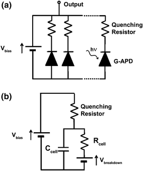
(a) Simplified electric structure of a SiPM composed of several G-APDs in series with a quenching resistor. (b) Equivalent circuit of a single cell when the device is on (a bias voltage V bias is applied) and is detecting photons. The capacitor C cell initially charged at V bias discharges through R cell dropping the bias voltage to V breakdown. The avalanche process is quenched via the quenching resistor and then the device is recharged
Figure 3
Figure 3
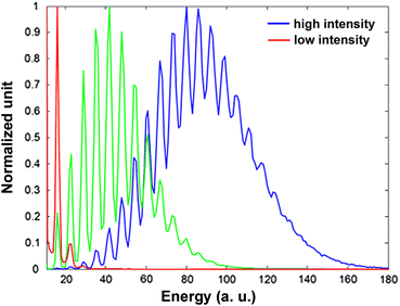
Pulse height spectra from a 1 × 1 mm2 Hamamatsu MPPC S10362-11-025C acquired for three different light intensities (the red and blue curves correspond to the lowest and strongest intensities, respectively) showing peaks corresponding to different numbers of photoelectrons generated
Figure 4
Figure 4
(a) Variation of gain as a function of bias voltage for a 1 × 1 mm2 SiPM with 400 cells, at different temperatures (from left to right: −25, −15, −5, 5, 15, and 25 °C) Piemonte et al. © 2008 IEEE. (b) Gain as a function of overvoltage for different temperatures for a 1 × 1 mm2 SensL SPM. Ramilli © 2008 IEEE
Figure 5
Figure 5
(a) PDE spectra for different overvoltages (10, 15, and 20%) acquired with a 1 × 1 mm2 SiPM (STMicroelectronics) with 289 cells and a fill factor of 48%. Mazillo et al. © 2009 IEEE. (b) PDE as a function of temperature for different overvoltages (10, 15, and 20%) for the same device as (a). Mazillo et al. © 2009 IEEE
Figure 6
Figure 6
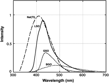
Emission spectra for scintillators commonly used in PET: sodium iodide (NaI(Tl)), lutetium oxyorthosilicate (LSO), gadolinium silicate (GSO), bismuth germanate (BGO). Melcher et al. © 1992 IEEE
Figure 7
Figure 7
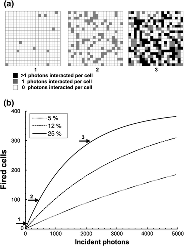
(a) Representation of a 400-cell SiPM at different light levels that results in (from left to right) 10, 100 and 300 cells firing. The grey scale indicates the number of photons interacting per cell and was calculated from Eq. (3), for a PDE of 25%. (b) Number of fired cells vs. number of incident photons: illustration of Eq. (3) for a SiPM with 400 cells and different PDE values (5, 12, and 25%)
Figure 8
Figure 8
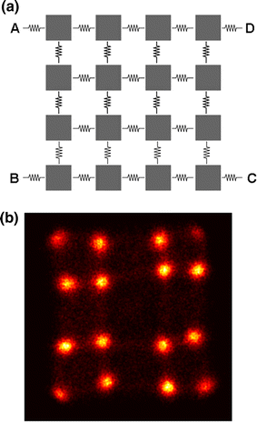
(a) Resistive network for a 4 × 4 SiPM array. (b) Crystal map acquired with a 22Na source irradiating a 4 × 4 array of 1.5 × 1.5 × 20 mm3 LSO scintillator crystals coupled to the SiPM array shown in Fig. 10a
Figure 9
Figure 9
(a) 22Na pulse height spectrum acquired at 23 °C with a 2 × 2 × 10 mm3 polished LSO crystal coupled to a 5 × 5 mm2 PS-SiPM (RMD Inc). Data courtesy of Jeffrey Schmall, UC Davis. (b) Energy resolution vs. bias voltage for a 5 × 5 mm2 PS-SiPM (RMD Inc) coupled to a 5 × 5 × 3 mm3 LSO crystal. McClish et al.
Figure 10
Figure 10
SiPM response as a function of energy for different bias voltages. Values are normalized to the response at 122 keV (57Co). Data were acquired with a 1 × 1 mm2 SiPM with 3600 cells. Non-linearity worsens with increasing bias voltage, as for a given incident light level, more cells fire (increased Geiger discharge probability) and saturation occurs earlier
Figure 11
Figure 11
(a) 5 × 5 mm2 PS-SiPM (RMD Inc.). (b) Crystal map obtained with 5 × 5 mm2 PS-SiPMs coupled to a 6 × 6 array of 0.5 × 0.5 × 5 mm3 LYSO crystals. All crystals can be easily resolved. McClish et al.
Figure 12
Figure 12
(a) DOI-encoding detectors. From left to right: offset crystal layers; different crystal layers; dual-ended readout. In each case, SiPM arrays could be utilized as the photodetector. (b) Prototype of a dual-head scanner with three module layers. Each layer is composed of a continuous LSO crystal coupled to a SiPM array. The thickness of the crystal defines the DOI resolution. Moehrs et al.
Figure 13
Figure 13
(a) MRI phantom images acquired with a gradient echo T2* sequence. Hong et al. In red: horizontal profile. In blue: vertical profile. (b) Vertical profile acquired without the PET detector. (c) Horizontal profile acquired without the PET detector. (d) Vertical profile acquired with the PET detector inside the bore. (e) Horizontal profile acquired with the PET detector inside the bore. Adapted from Hong et al. © 2008 IEEE

References

    1. Amplification Technologies. http://www.amplificationtechnologies.com/.
    1. Anfimov, N., I. Chirikov-Zorin, A. Dovlatov, O. Gavrishchuk, A. Guskov, N. Khovanskiy, Z. Krumshtein, R. Leitner, G. Meshcheryakov, A. Nagaytsev, A. Olchevski, T. Rezinko, A. Sadovskiy, Z. Sadygov, I. Savin, V. Tchalyshev, I. Tyapkin, G. Yarygin, and F. Zerrouk. Novel micropixel avalanche photodiodes (MAPD) with super high pixel density. Nucl. Instrum. Methods Phys. Res. A., 2010. doi:10.1016/j.nima.2010.07.003.
    1. Balcerzyk M, Moszynski M, Kapusta M, Wolski D, Pawelke J, Melcher CL. YSO, LSO, GSO and LGSO. A study of energy resolution and nonproportionality. IEEE Trans. Nucl. Sci. 2000;47:1319–1323. doi: 10.1109/23.872971. - DOI
    1. Bar-Shalom R, Yefremov N, Guralnik L, Gaitini D, Frenkel A, Kuten A, Altman H, Keidar Z, Israel O. Clinical performance of PET/CT in evaluation of cancer: additional value for diagnostic imaging and patient management. J. Nucl. Med. 2003;44:1200–1209. - PubMed
    1. Bergeron M, Cadorette J, Beaudoin J-F, Lepage MD, Robert G, Selivanov V, Tetrault M-A, Viscogliosi N, Norenberg JP, Fontaine R, Lecomte R. Performance evaluation of the LabPET APD-based digital PET scanner. IEEE Trans. Nucl. Sci. 2009;56:10–16. doi: 10.1109/TNS.2008.2010257. - DOI

LinkOut - more resources