

Molecular printing
- PMID: 21378889
- PMCID: PMC3936963
- DOI: 10.1038/nchem.258
Molecular printing
Abstract
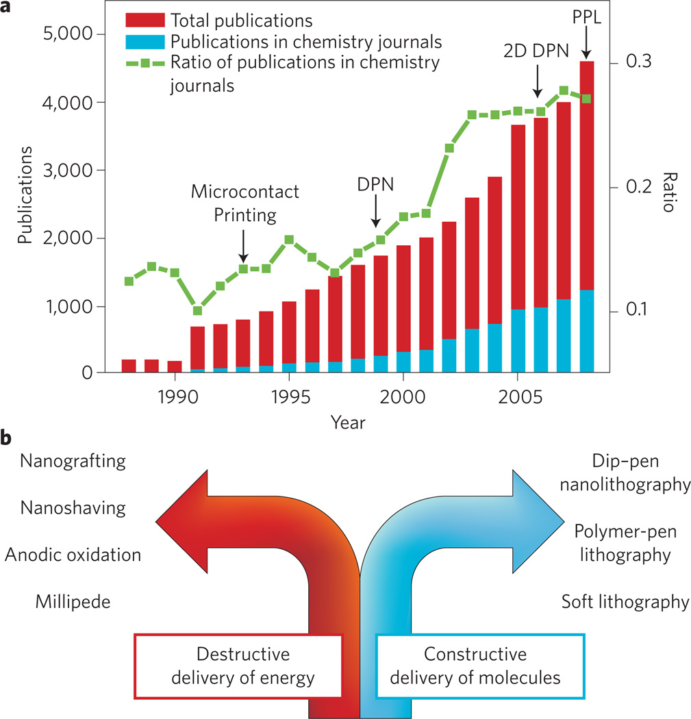
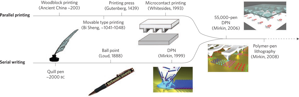
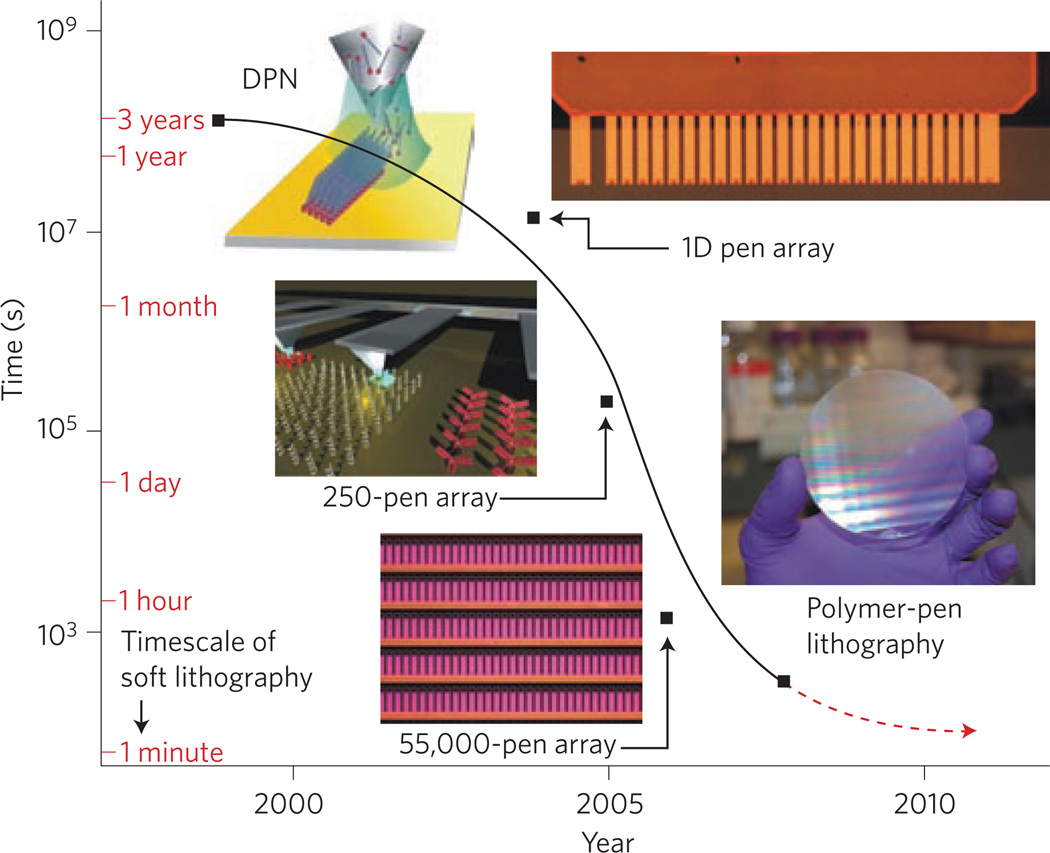
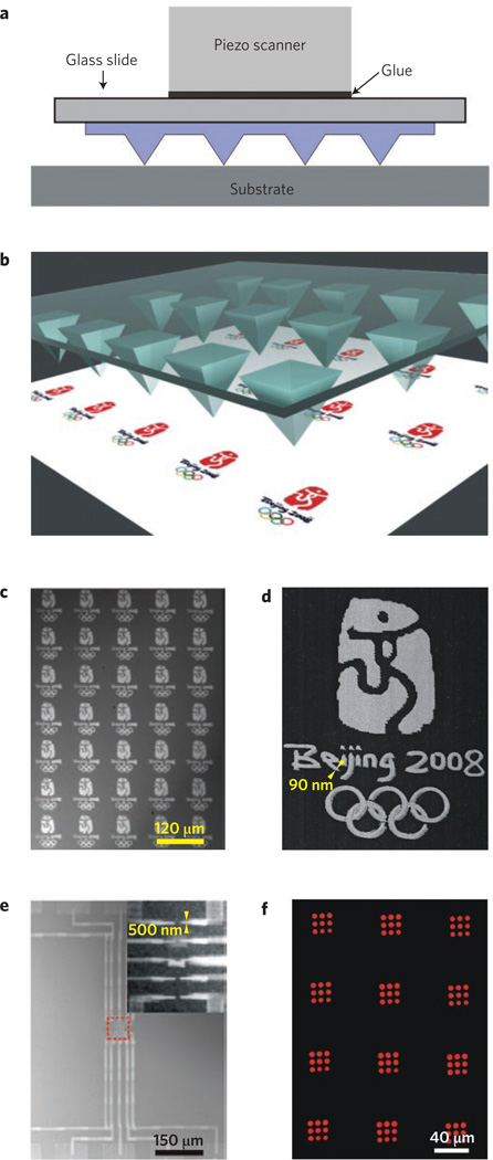
Molecular printing techniques, which involve the direct transfer of molecules to a substrate with submicrometre resolution, have been extensively developed over the past decade and have enabled many applications. Arrays of features on this scale have been used to direct materials assembly, in nanoelectronics, and as tools for genetic analysis and disease detection. The past decade has witnessed the maturation of molecular printing led by two synergistic technologies: dip-pen nanolithography and soft lithography. Both are characterized by material and substrate flexibility, but dip-pen nanolithography has unlimited pattern design whereas soft lithography has limited pattern flexibility but is low in cost and has high throughput. Advances in DPN tip arrays and inking methods have increased the throughput and enabled applications such as multiplexed arrays. A new approach to molecular printing, polymer-pen lithography, achieves low-cost, high-throughput and pattern flexibility. This Perspective discusses the evolution and future directions of molecular printing.
Figures
Similar articles
-
Electrostatic nanolithography in polymers using atomic force microscopy.Nat Mater. 2003 Jul;2(7):468-72. doi: 10.1038/nmat926. Nat Mater. 2003. PMID: 12819776
-
Multiplexed protein arrays enabled by polymer pen lithography: addressing the inking challenge.Angew Chem Int Ed Engl. 2009;48(41):7626-9. doi: 10.1002/anie.200902649. Angew Chem Int Ed Engl. 2009. PMID: 19731290 Free PMC article. No abstract available.
-
Hard Transparent Arrays for Polymer Pen Lithography.ACS Nano. 2016 Mar 22;10(3):3144-8. doi: 10.1021/acsnano.6b00528. Epub 2016 Mar 1. ACS Nano. 2016. PMID: 26928012 Free PMC article.
-
Evolution of Dip-Pen Nanolithography (DPN): From Molecular Patterning to Materials Discovery.Chem Rev. 2020 Jul 8;120(13):6009-6047. doi: 10.1021/acs.chemrev.9b00725. Epub 2020 Apr 22. Chem Rev. 2020. PMID: 32319753 Review.
-
Development of Dip-Pen Nanolithography (DPN) and Its Derivatives.Small. 2019 May;15(21):e1900564. doi: 10.1002/smll.201900564. Epub 2019 Apr 12. Small. 2019. PMID: 30977978 Review.
Cited by
-
Beam pen lithography as a new tool for spatially controlled photochemistry, and its utilization in the synthesis of multivalent glycan arrays.Chem Sci. 2014 May 1;5(5):2023-2030. doi: 10.1039/c3sc53315h. Epub 2014 Feb 4. Chem Sci. 2014. PMID: 34113434 Free PMC article.
-
High-efficacy subcellular micropatterning of proteins using fibrinogen anchors.J Cell Biol. 2021 Feb 1;220(2):e202009063. doi: 10.1083/jcb.202009063. J Cell Biol. 2021. PMID: 33416860 Free PMC article.
-
Design of surface modifications for nanoscale sensor applications.Sensors (Basel). 2015 Jan 14;15(1):1635-75. doi: 10.3390/s150101635. Sensors (Basel). 2015. PMID: 25594599 Free PMC article. Review.
-
Nano-confined crystallization of organic ultrathin nanostructure arrays with programmable geometries.Nat Commun. 2019 Sep 2;10(1):3912. doi: 10.1038/s41467-019-11883-6. Nat Commun. 2019. PMID: 31477721 Free PMC article.
-
Femtomolar hydrogen sulfide detection via hybrid small-molecule nano-arrays.Nat Commun. 2024 Dec 30;15(1):10831. doi: 10.1038/s41467-024-55123-y. Nat Commun. 2024. PMID: 39738008 Free PMC article.
References
-
- Pease RFW. Nanolithography and its prospects as a manufacturing technology. J. Vac. Sci. Technol. B. 1992;10:278–285.
-
- Rai-Choudhury P, editor. Handbook of Microlithography, Micromachining and Microfabrication. Vol. 1. SPIE Press; 1997.
-
- Chou SY, Krauss PR, Renstrom PJ. Imprint lithography with 25-nanometer resolution. Science. 1996;272:85–87.
-
- Wouters D, Hoeppener S, Schubert US. Local probe oxidation of self-assembled monolayers: Templates for the assembly of functional nanostructures. Angew. Chem. Int. Ed. 2009;48:1732–1739. - PubMed
-
- Xia Y, Whitesides GM. Soft lithography. Angew. Chem. Int. Ed. 1998;37:550–575. - PubMed
Publication types
MeSH terms
Substances
Grants and funding
LinkOut - more resources
Full Text Sources
Other Literature Sources
Miscellaneous
