

Hf-based high-k materials for Si nanocrystal floating gate memories
- PMID: 21711676
- PMCID: PMC3211225
- DOI: 10.1186/1556-276X-6-172
Hf-based high-k materials for Si nanocrystal floating gate memories
Abstract
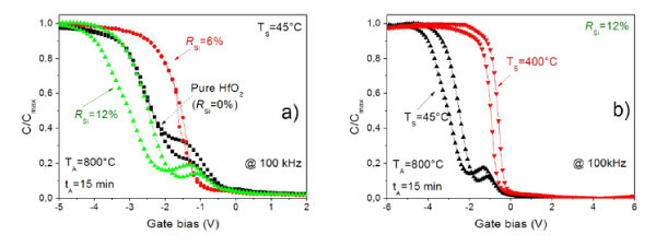
Pure and Si-rich HfO2 layers fabricated by radio frequency sputtering were utilized as alternative tunnel oxide layers for high-k/Si-nanocrystals-SiO2/SiO2 memory structures. The effect of Si incorporation on the properties of Hf-based tunnel layer was investigated. The Si-rich SiO2 active layers were used as charge storage layers, and their properties were studied versus deposition conditions and annealing treatment. The capacitance-voltage measurements were performed to study the charge trapping characteristics of these structures. It was shown that with specific deposition conditions and annealing treatment, a large memory window of about 6.8 V is achievable at a sweeping voltage of ± 6 V, indicating the utility of these stack structures for low-operating-voltage nonvolatile memory devices.
Figures


References
-
- Aaron VY, Leburton JP. Flash memory: towards single-electronics. IEEE Potentials. 2002;21:35. doi: 10.1109/MP.2002.1044216. - DOI
-
- Tiwari S, Rana F, Hanafi H, Hartstein A, Crabbe EF, Chan K. A silicon nanocrystals based memory. Appl Phys Lett. 1996;68:1377. doi: 10.1063/1.116085. - DOI
-
- Hanafi HI, Tiwari S, Khan I. Fast and long retention-time nano-crystal memory. IEEE Trans Electron Devices. 1996;43:1553. doi: 10.1109/16.535349. - DOI
-
- King YC, King TJ, Hu C. Charge-trap memory device fabricated by oxidation of Si1-x Gex. IEEE Trans Electron Devices. 2001;48:696. doi: 10.1109/16.915694. - DOI
-
- Ng CY, Chen TP, Ding L, Fung S. Memory characteristics of MOSFETs with densely stacked silicon nanocrystal layers in the gate oxide synthesized by low-energy ion beam. IEEE Electron Device Lett. 2006;27:231. doi: 10.1109/LED.2006.871183. - DOI
LinkOut - more resources
Full Text Sources
Research Materials
Miscellaneous
