. 2011 Sep;243(3):273-83.
doi: 10.1111/j.1365-2818.2011.03501.x. Epub 2011 Jul 19.

Silicon nitride windows for electron microscopy of whole cells

Affiliations

Silicon nitride windows for electron microscopy of whole cells

E A Ring et al. J Microsc. 2011 Sep.

Abstract

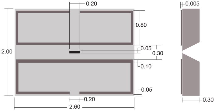
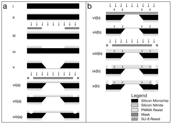
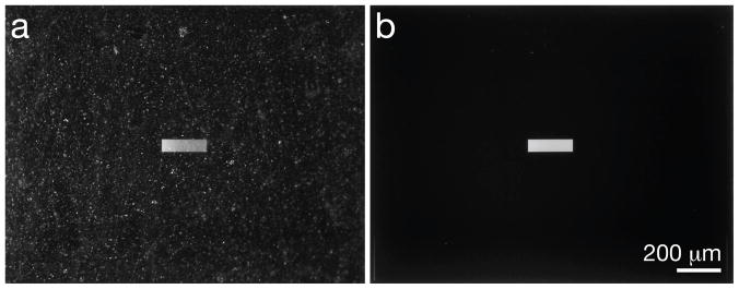
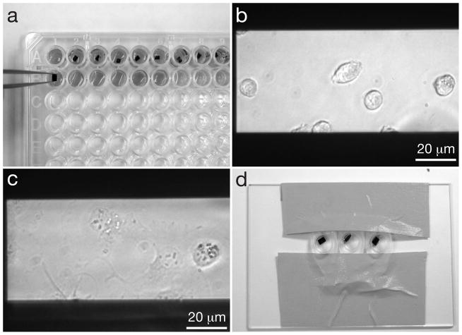
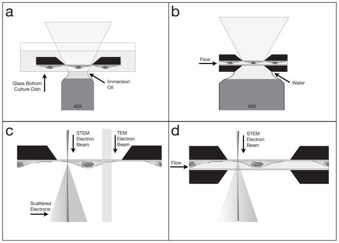
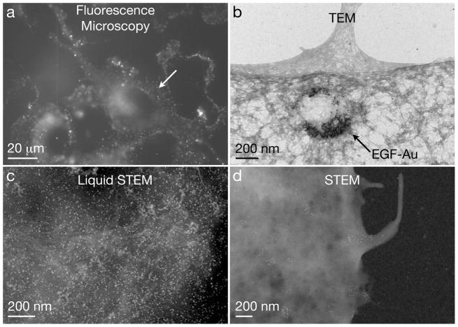
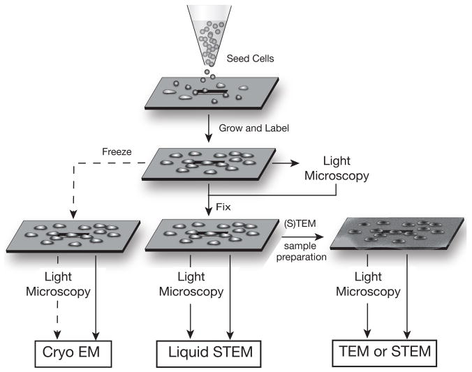
Silicon microchips with thin, electron transparent silicon nitride windows provide a sample support that accommodates both light-, and electron microscopy of whole eukaryotic cells in vacuum or liquid, with minimum sample preparation steps. The windows are robust enough that cellular samples can be cultured directly onto them, with no addition of a supporting film, and there is no need to embed or section the sample, as is typically required in electron microscopy. By combining two microchips, a microfluidic chamber can be constructed for the imaging of samples in liquid in the electron microscope. We provide microchip design specifications, a fabrication outline, instructions on how to prepare the microchips for biological samples, and examples of images obtained using different light and electron microscopy modalities. The use of these microchips is particularly advantageous for correlative light and electron microscopy.


Figures

Fig. 1
Fig. 1
The design of the spacer microchip. Both the top view and the side-view cross-section are shown. All dimensions are in mm. The microchip had a width of 2.00 mm, a length of 2.60 mm, and a thickness of 0.30 mm. The tolerances were ± 10 μm. The black area in the middle indicates the 50 nm thick silicon nitride (SiN) window. A patterned spacer is shown in dark grey, providing a flow channel over the SiN window.
Fig. 2
Fig. 2
Schematic of the workflow of the fabrication of (a) the base microchips and (b) the spacer microchips. The arrows indicate lithographic exposure. Drawings not to scale.
Fig. 3
Fig. 3
Photographs showing the difference between coated and clean microchips. (a) A microchip with a protective resist coat, covered in debris is shown. (b) The same microchip after washing with acetone, ethanol, and water.
Fig. 4
Fig. 4
Seeding cells onto microchips and labeling the cells. (a) Microchips in a 96 well plate, where they will be seeded with cells, and the cells will be fixed. Note the orientation of the tweezers gripping microchips by their sides and not their top surfaces. Tweezers with a teflon coated flat tips are recommended. (b) COS7 cells on windows after ~5 minutes of incubation. (c) COS7 cells that have adhered to a window, after ~1 hour of incubation. (d) Microchips in labeling device are inclined against a drop of labeling solution to reduce the amount of non-specifically bound label on the sample.
Fig. 5
Fig. 5
Schematics showing different ways microchips can be used for imaging. Images not to scale. (a) The microchip can be imaged in liquid in a standard dish with light microscopy (LM). (b) Two microchips enclosing a sample in liquid can be imaged with LM. (c) A dry sample on a microchip can be imaged with transmission electron microscopy (TEM), or the scanning TEM (STEM). (d) Two microchips enclosing a cell in liquid can be imaged with STEM; thin samples can be imaged in liquid TEM as well. Drawings not to scale.
Fig. 6
Fig. 6
Examples of micrographs of cellular samples on microchips obtained with different microscopy modalities. (a) Fluorescence image showing epidermal growth factor (EGF)-quantum dot (QD) labeled COS7 fibroblast cells in saline water. Image with permission from (Dukes et al., 2010a). (b) TEM image of EGF-Au nanoparticles in a vesicle in a fixed and dried COS7 cell. (c) Liquid STEM image recorded at the location of the arrow in (a). Individual quantum dots are visible on a background of biological material. (d) Dry STEM image of EGF-QD labels on the edge of a COS7 cell.
Fig. 7
Fig. 7
Diagram illustrating the versatility of the silicon microchip support for whole mount cell samples for imaging with different modalities. Cells are seeded onto a clean poly-L-lysine coated microchip, and grown and labeled (if needed) directly on the support. Live cells can be imaged with LM. The cells can then be fixed, or frozen (freezing was not yet tested and this branch in the schematics is, therefore, indicated with a dashed line). Fixed cells can undergo additional sample preparation steps for EM processing such as staining, dehydrating and evaporative coating, as needed. This sample preparation system permits multiple samples to be prepared under the same conditions, and efficiently processed for cryo EM, liquid STEM, TEM, and dry STEM. Thin biological samples can also be imaging with liquid TEM. The cells can be imaged at different stages with LM enabling correlative imaging studies to be performed. Drawings not to scale.

References

    1. Agronskaia AV, Valentijn JA, van Driel LF, Schneijdenberg CT, Humbel BM, van Bergen en Henegouwen PM, Verkleij AJ, Koster AJ, Gerritsen HC. Integrated fluorescence and transmission electron microscopy. J Struct Biol. 2008;164:183–189. - PubMed
    1. Barcena M, Koster AJ. Electron tomography in life science. Semin Cell Dev Biol. 2009;20:920–930. - PMC - PubMed
    1. Bozzola JJ, Russell LD. Electron Microscopy Principles and Techniques for Biologists. Jones and Barlett Publishers; Boston: 1999.
    1. Braet F, De Zanger R, Wisse E. Drying cells for SEM, AFM and TEM by hexamethyldisilazane: a study on hepatic endothelial cells. J Micros. 1997;186:84–87. - PubMed
    1. Ciarlo DR. Silicon nitride thin windows for biomedical microdevices. Biomed Microdev. 2002;4:63–68.

Publication types