. 2010 May;9(3):269-280.
doi: 10.1109/TNANO.2009.2031807.

Design and Implementation of Functional Nanoelectronic Interfaces With Biomolecules, Cells, and Tissue Using Nanowire Device Arrays

Affiliations

Design and Implementation of Functional Nanoelectronic Interfaces With Biomolecules, Cells, and Tissue Using Nanowire Device Arrays

Brian P Timko et al. IEEE Trans Nanotechnol. 2010 May.

Abstract

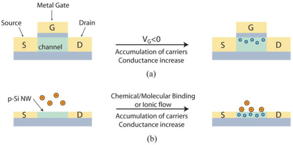
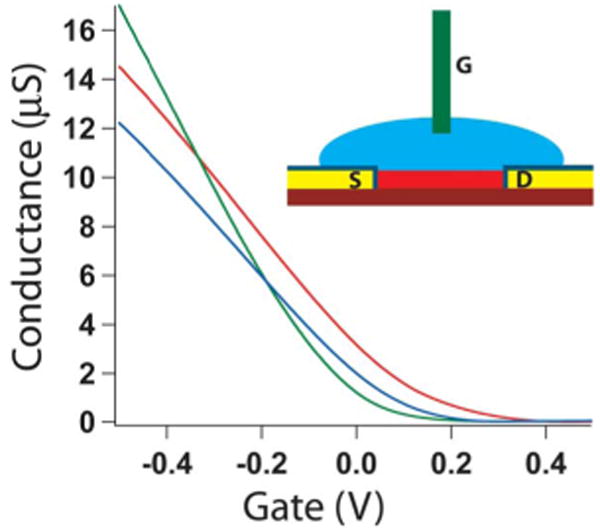
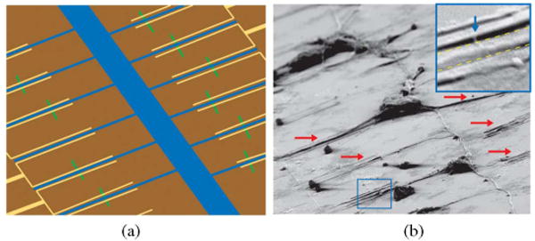
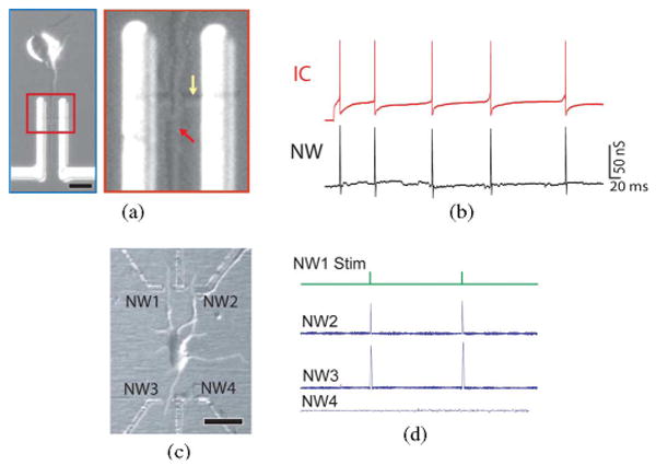
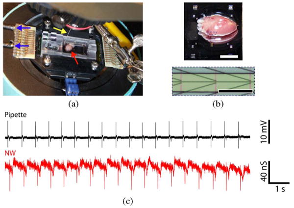
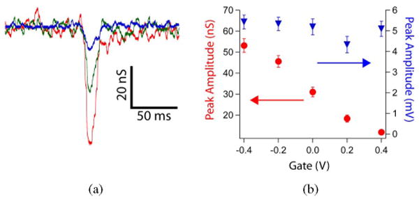
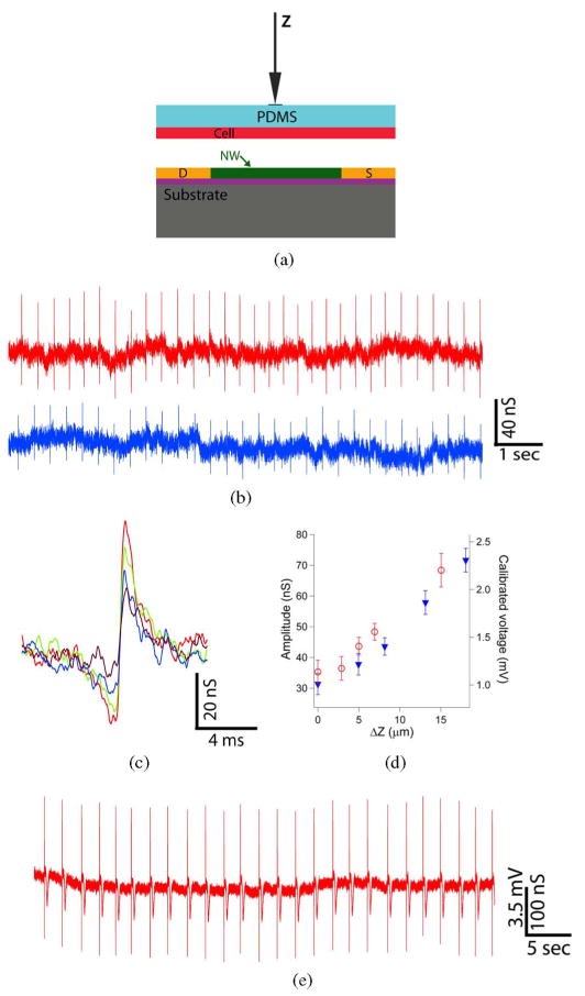
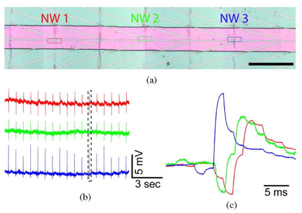
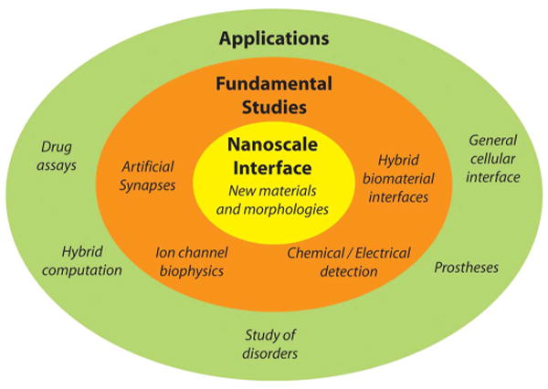
Nanowire FETs (NWFETs) are promising building blocks for nanoscale bioelectronic interfaces with cells and tissue since they are known to exhibit exquisite sensitivity in the context of chemical and biological detection, and have the potential to form strongly coupled interfaces with cell membranes. We present a general scheme that can be used to assemble NWs with rationally designed composition and geometry on either planar inorganic or biocompatible flexible plastic surfaces. We demonstrate that these devices can be used to measure signals from neurons, cardiomyocytes, and heart tissue. Reported signals are in millivolts range, which are equal to or substantially greater than those recorded with either planar FETs or multielectrode arrays, and demonstrate one unique advantage of NW-based devices. Basic studies showing the effect of device sensitivity and cell/substrate junction quality on signal magnitude are presented. Finally, our demonstrated ability to design high-density arrays of NWFETs enables us to map signal at the subcellular level, a functionality not enabled by conventional microfabricated devices. These advances could have broad applications in high-throughput drug assays, fundamental biophysical studies of cellular function, and development of powerful prosthetics.


Figures

Fig. 1
Fig. 1
(a) Schematic of a p-type planar FET device, where S, D, and G correspond to source, drain and gate electrodes, respectively. (b) Schematic of electrically based sensing using a p-type NWFET, where binding of a charged biological or chemical species to the chemically modified gate dielectric is analogous to applying a voltage using a gate electrode.
Fig. 2
Fig. 2
(a) Schematic illustration of a single virus binding and unbinding to the surface of an NWFET modified with antibody receptors. (b) Conductance versus time data recorded from a single device modified with antiinfluenza type A antibody. (c) Optical data recorded simultaneously with conductance data in (b). Combined bright-field and fluorescence images correspond to time points 1–6 indicated in the conductance data; virus appears as a red dot in the images. The white arrow in image 1 highlights the position of the NW, and the red arrow indicates the position of a single virus. Images are 8 × 8 μm. Adapted from [35] (National Academy of Sciences, copyright 2004).
Fig. 3
Fig. 3
(a) Schematic illustration of an NWFET configured as a protein sensor with antibody receptors (blue). (b) Complementary sensing of PSA using p-type (NW1) and n-type (NW2) devices. Points 1–5 correspond to the addition of PSA solutions of (1, 2) 0.9 ng/mL, (3) 9 pg/mL, (4) 0.9 pg/mL, and (5) 5 ng/mL. Adapted from [36] (Nature Publishing Group, copyright 2005).
Fig. 4
Fig. 4
Schematic diagram outlining unique advantages of bottom-up NW assembly, including (a) nanotopographic morphology, (b) ability to assemble devices on flexible, transparent substrates, (c) assembly of distinct NW materials on the same chip, and (d) high spatial resolution of NW devices, where S and D correspond to source and drain electrodes.
Fig. 5
Fig. 5
Conductance versus water-gate voltage for three representative NWFET devices. Inset: Scheme representing experimental setup, which includes: (red) NW, (yellow/navy) passivated contact electrodes, (blue) electrolyte solution, and (green) Ag/AgCl reference/gate electrode.
Fig. 6
Fig. 6
NW/neuron interfaces. (a) Schematic of interconnected neuron motif and (b) SEM image of fixed neurons exhibiting a neural network where multiple neurites are interfaced with (red arrows) NW devices. Inset: Zoom depicting an axon (denoted by yellow dotted lines) guided between source and drain electrodes across an NWFET (highlighted by blue arrow).
Fig. 7
Fig. 7
(a) Optical image of a cortical neuron aligned across an NWFET; scale bar is 10 μm. Inset: High-resolution image of region where (red arrow) axon crosses (yellow arrow) an NW. (b, red trace) IC potential of an aligned cortex neuron (after 6 days in culture) during stimulation with a 500-ms-long current injection step of 0.1 nA; (b, black trace) time-correlated signal from axon measured using a p-type NWFET. (c) Optical image of a cortical neuron interfaced to three of the four functional NWFETs in an array; scale bar is 20 μm. (d) Trace of pulses applied to NW1 for antidromic stimulation of the neuron. The response was measured by the NW–dendrite junctions at NW2 and NW3. Adapted from [58] (American Association for the Advancement of Science, copyright 2006).
Fig. 8
Fig. 8
NW/heart interfaces. (a) Experimental setup showing heart on NWFET chip in temperature regulated cell. Arrows show (red) position of heart, (yellow) Ag/AgCl reference electrode, and (blue) source/drain interconnect wires. (b, top) Magnified image of heart on surface of planar chip; scale bar is 4 mm. (Bottom) Zoom of dotted region in upper image showing three pairs of NWFETs; scale bar is 150 μm. (c) Simultaneous recordings from (black trace) a glass pipette and (red trace) an NW device. Adapted from [56] (American Chemical Society, copyright 2009).
Fig. 9
Fig. 9
(a) Expansion of single fast transients recorded from a heart for (red) Vg = −0.4 V, (green) 0 V, and (blue) 0.4 V. (b) Plots of (red) peak conductance amplitude and (blue) calibrated peak voltage amplitude versus Vg for same experiment shown in a. Adapted from [56] (American Chemical Society, copyright 2009).
Fig. 10
Fig. 10
(a) (Yellow arrow) Heart located underneath bent substrate with NWFETs on the lower concave face of the substrate. (b, left) Top-down photograph of same system, which enables overall registration between heart and lithographically defined markers on the substrate. (Right) Optical image taken with same system showing features on the heart surface versus position of individual NW devices, which are located along the central horizontal axis. Scale bar is 150 μm. (c) Recorded conductance data from an NWFET in the configuration shown in (a). Adapted from [56] (American Chemical Society, copyright 2009).
Fig. 11
Fig. 11
(A) NWFET chip, where NW devices are located at the central region of chip. The visible linear features (gold) correspond to NW contacts and interconnect metal. Zoom-in showing a source (S) and two drain (D) electrodes connected to a vertically oriented NW (blue arrow) define two NWFETs. (b) Cardiomyocytes cultured on thin flexible pieces of PDMS, where (green) one piece is being removed with tweezers. (c) PDMS substrate with cultured cells oriented over the device region of the NWFET chip. The green needle-like structure indicates the probe used to both manipulate the PDMS/cell substrate to specific NW device locations. (d) Schematic of (black arrow) a cardiomyocyte oriented over (green arrow) an NW device. Adapted from [73] (National Academy of Sciences, copyright 2009).
Fig. 12
Fig. 12
(a) Patch of (red dashed oval) beating cells over (yellow arrow) an NWFET; scale bar is 40 μm. (b) Conductance versus time signals recorded from this cell patch. (c) Distinct patch of (red dashed oval) beating cells over (yellow arrow) an NW device; scale bar is 20 μm. (d) Conductance versus time signals recorded from the cells. Adapted from [73] (National Academy of Sciences, copyright 2009).
Fig. 13
Fig. 13
(a) Schematic illustrating displacement (Z) of the PDMS/cell substrate with respect to an NWFET device. (b) Two representative traces recorded with same device for ΔZ values of (blue) 8.2 μm and (red) 18.0 μm. (c) High-resolution comparison of single peaks recorded with ΔZ values of (purple) 0, (blue) 8.2 (blue), (green) 13.1, and (red) 18.0. (d) Summary of the recorded conductance signals and calibrated voltages versus ΔZ, where the open red circles (filled blue triangles) were recorded for increasing (decreasing) ΔZ. (e) Data recorded in distinct experiment at ΔZ close to cell failure. Adapted from [73] (National Academy of Sciences, copyright 2009).
Fig. 14
Fig. 14
(a) Optical micrograph showing three NWFET devices (NW1, NW2, and NW3) in a linear array, where pink indicates the area with exposed NW devices; scale bar is 150 μm. (b) Representative conductance versus time signals recorded simultaneously from NW1, NW2, and NW3. (c) High-resolution comparison of the temporally correlated peaks highlighted by the black dashed box in (b). Adapted from [73] (National Academy of Sciences, copyright 2009).
Fig. 15
Fig. 15
Overview of a bottom-up paradigm for NW nanobioelectronic interfaces.

Similar articles

Cited by

References

    1. Hille B. Ion Channels of Excitable Membranes. Sunderland, MA: Sinauer; 2001.
    1. Zipes DP, Jalife J. Cardiac Electrophysiology: From Cell to Bedside. Philadelphia, PA: Saunders; 2004. pp. 169–253.
    1. Dhein S, Mohr FW, Delmar M. Practical Methods in Cardiovascular Research. Berlin, Germany: Springer-Verlag; 2005. pp. 215–453.
    1. Davie JT, Kole MHP, Letzkus JJ, Rancz EA, Spruston N, Stuart GJ, Häusser M. Dendritic patch-clamp recording. Nat Protocols. 2006;1(3):1235–1247. - PMC - PubMed
    1. Zochowski M, Wachowiak M, Falk CX, Cohen LB, Lam YW, Antic S, Zecevic D. Concepts in imaging and microscopy - Imaging membrane potential with voltage-sensitive dyes. Biol Bull. 2000;198(1):1–12. - PubMed

LinkOut - more resources