doi: 10.1016/j.bios.2011.07.025.
Epub 2011 Jul 23.
Multiplexed SOI BioFETs
Affiliations
- PMID: 21820303
- PMCID: PMC3235496
- DOI: 10.1016/j.bios.2011.07.025
Item in Clipboard
Multiplexed SOI BioFETs
Biosens Bioelectron.
.
Abstract
Nanoscale Field Effect Transistors have emerged as a promising technology for ultrasensitive, unlabeled diagnostic applications. However, their use as quantitative sensors has been problematic because of the need for individual sensor calibration. In this work we demonstrate an internal calibration scheme for multiplexed nanoribbon field effect sensors by utilizing the initial current rates rather than end point detection. A linear response is observed consistent with initial binding kinetics. Moreover, we are able to show that top-down fabrication techniques yield reproducible device results with minimal fluctuations, enabling internal calibration.
Copyright © 2011 Elsevier B.V. All rights reserved.
Figures

a) Device schematic b) Electrical characteristics, Ids-Vgs, and gm-Vgs, of a typical nanoribbon device, c) threshold voltage distribution of nanoribbon devices across a 4″ wafer. Each data point is a 5×5 mm die containing up to 8 devices. The inset shows approximate die positions on the wafer. Notation a) and b) in the die label refers to the lower and the upper half of a 10 × 5 mm die. (10,3) is a center column die.
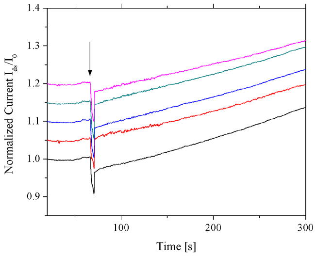
Normalized current response of 5 functionalized devices on the same chip upon addition of CA15.3, measured simultaneously. I0 is the baseline current for a given device prior to analyte addition. The arrow indicates injection of the analyte solution. Time traces are intentionally offset by 0.05 along the y-axis for visual clarity.

Initial current rate of five devices shown in Fig 2 as a function of both baseline currents and device solution transconductances at Vbackgate=−3V and Vsol=0V. Error bars are approximately the size of the data points. The relative standard deviations for initial current rates, baseline currents and tranconductances are 0.7%, 0.3% and 0.6%, respectively. Both fits are linear (y=kx), shown on a log-log scale for clarity.

Calibration curves for (a) PSA and (b) CA15.3 show linear device response in the clinically relevant range of analytes. Red data point represents a blind measurement.
References
Publication types
MeSH terms
Substances
Grants and funding
LinkOut - more resources
Full Text Sources
Other Literature Sources