Review
. 2011 Sep 7;56(17):R145-82.
doi: 10.1088/0031-9155/56/17/R01. Epub 2011 Aug 9.

SPECT detectors: the Anger Camera and beyond

Affiliations
Review

SPECT detectors: the Anger Camera and beyond

Todd E Peterson et al. Phys Med Biol. .

Abstract

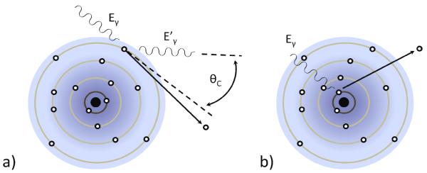
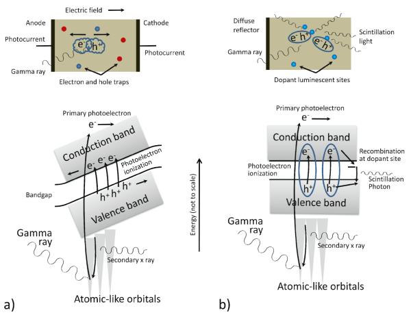
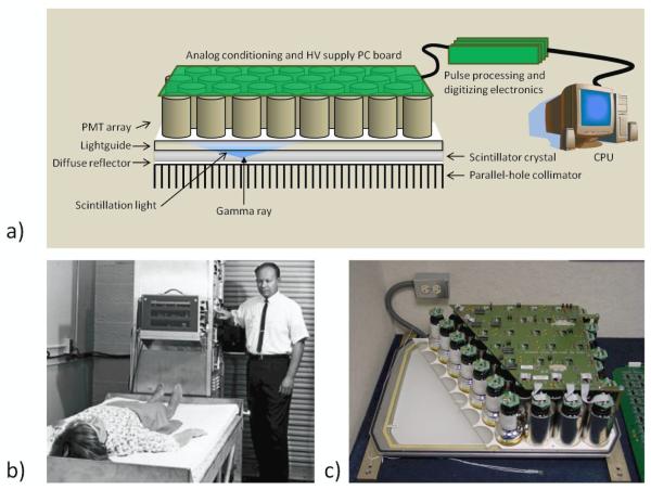
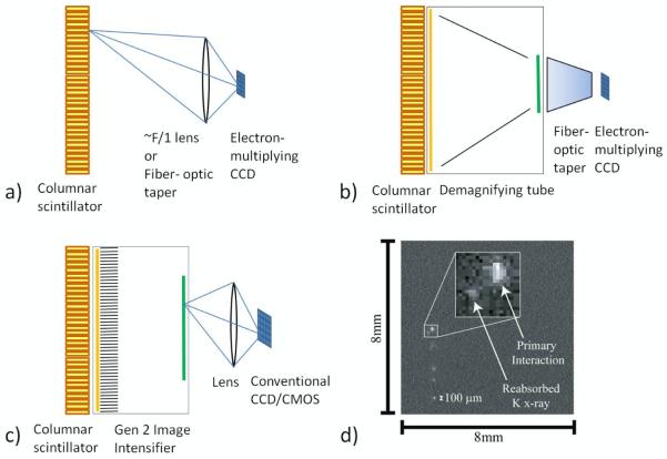
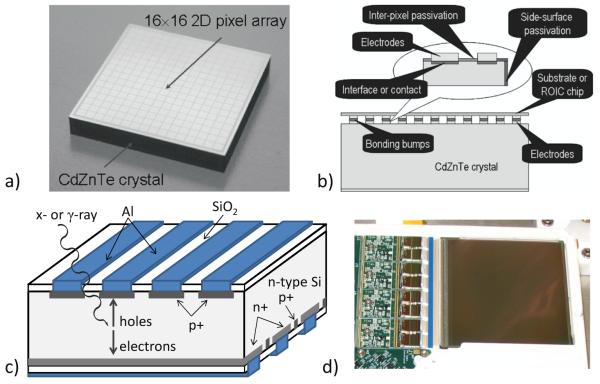
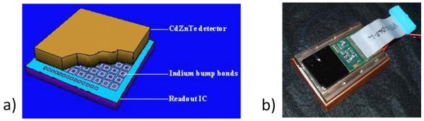
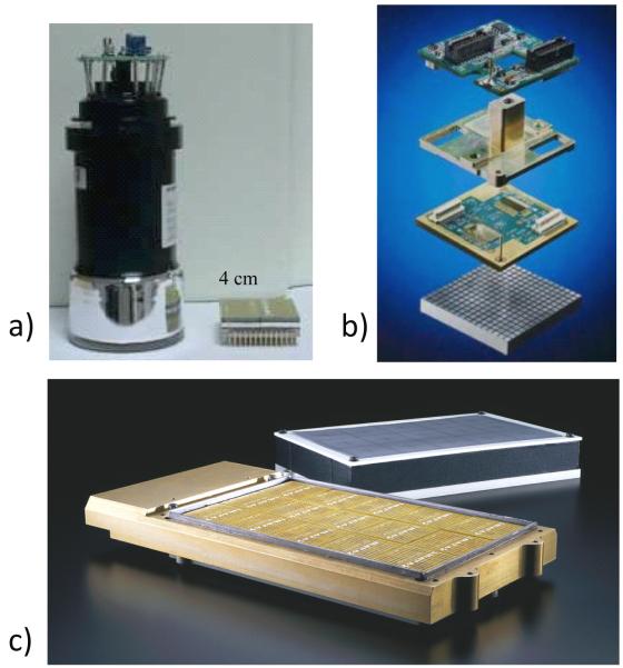
The development of radiation detectors capable of delivering spatial information about gamma-ray interactions was one of the key enabling technologies for nuclear medicine imaging and, eventually, single-photon emission computed tomography (SPECT). The continuous sodium iodide scintillator crystal coupled to an array of photomultiplier tubes, almost universally referred to as the Anger Camera after its inventor, has long been the dominant SPECT detector system. Nevertheless, many alternative materials and configurations have been investigated over the years. Technological advances as well as the emerging importance of specialized applications, such as cardiac and preclinical imaging, have spurred innovation such that alternatives to the Anger Camera are now part of commercial imaging systems. Increased computing power has made it practical to apply advanced signal processing and estimation schemes to make better use of the information contained in the detector signals. In this review we discuss the key performance properties of SPECT detectors and survey developments in both scintillator and semiconductor detectors and their readouts with an eye toward some of the practical issues at least in part responsible for the continuing prevalence of the Anger Camera in the clinic.
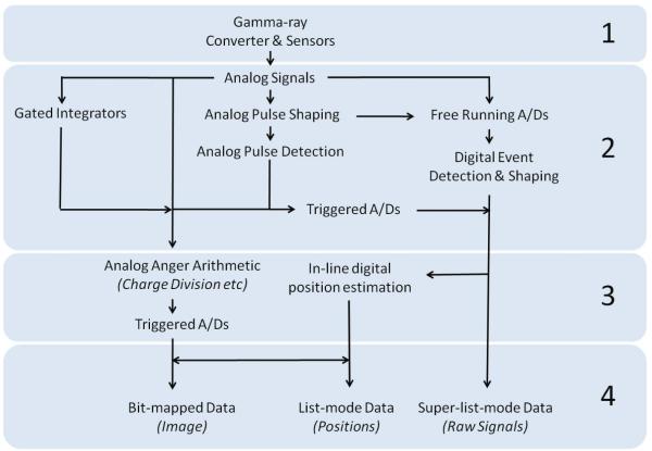

Figures

Figure 1
Figure 1
a) Schematic representation of the Compton-scatter interaction in which a gamma-ray photon transfers part of its energy to an a outer-shell electron (Eγ > Eγ ’). b) Schematic representation of a photoelectric interaction in which a gamma ray transfers all of its energy to the binding energy and residual kinetic energy of a core electron.
Figure 2
Figure 2
a) Representation of the photoelectric process in a direct-conversion material, showing the excitation of electron-hole pairs that drift in opposite directions under the influence of an externally applied electric field. The moving charge induces electrical signals on the electrodes that can be read out. b) A photoelectric interaction in a scintillator also creates electron-hole pairs, but in the absence of the applied field they stay together as loosely bound pseudoparticles known as excitons. The excitons diffuse to luminescent centers where they recombinne, emitting secondary scintillation photons in the process that can be read out using an appropriate light sensor.
Figure 3
Figure 3
a) The basic structure of the Anger Camera comprises a collimator, a monolithic scintillator crystal, a light guide that allows light to spread, and an array of photomultiplier tubes (PMTs) with related electronics. Position estimation was originally performed with analog circuitry; in current systems PMT outputs are digitized and all processing is digital. b) Hal Anger shown with early example of his camera being applied in a clinical setting (Reprinted by permission of the Society of Nuclear Medicine from: Nuclear Medicine Pioneer, Hal O. Anger, 1920–2005. J Nucl Med Technol. 2005; 33(4): 250-253). c) A cutaway of an actual camera (Courtesy of M. Wernick and J. Aarsvold).
Figure 4
Figure 4
Positioning results from a regular array of points projected on the face of an Anger Camera before (left) and after (right) processing to correct for systematic distortions characteristic of Anger Arithmetic. From (Villena et al., 2010)
Figure 5
Figure 5
a) A 48 × 48 scintillator array with 1-mm pitch. b) Raw image from resistive-readout of a Burle Planacon MA-PMT coupled to a NaI(Tl) scintillator array. c) X and Y projections of the 2D image shown in b). (Photo courtesy of A. Weisenberger, Jefferson Lab, while b) and c) are from (Popov et al., 2003).)
Figure 6
Figure 6
a) Top and b) cross-sectional SEM micrographs of a 1.3-mm thick microcolumnar CsI(Tl) film. (Courtesy of V. Nagarkar, RMD, Inc.)
Figure 7
Figure 7
a) Schematic drawing of a silicon drift detector. The electron collecting side is patterned with a set of concentric electrodes that create a horizontal drift field that guides the electron charge cloud to a very small collection anode. b) An array of hexagonal silicon drift detectors (Courtesy of Brookhaven Nationall Laboratory).
Figure 8
Figure 8
a) A schematic representation of a PSAPD showing the four contacts at the corners of the resistive layer with arrows indicating the charge division in the resistive layer. b) Raw flood image from PSAPD readout of a scintillator crystal array. The superposed white dots are from a simulation of the charge division process. From (Despres et al., 2007).
Figure 9
Figure 9
The principal CCD/CMOS SPECT camera geometries employing columnar scintillators and capable of photon counting: a) direct lens-coupled (or fiber-optics-taper-coupled) EMCCD system; b) demagnifying tube and fiber-optic-coupled EMCCD; and c) image-intensified and lens-coupled conventional CCD or CMOS camera. d) A single frame from an EMCCD showing a primary gamma-ray interaction along with a reabsorbed secondary x-ray (courtesy of B.W. Miller, Univ. of Arizona).
Figure 10
Figure 10
a) An example of a 2D pixel detector. b) In a pixel detector all electrodes can be bonded directly to the readout electronics. c) A schematic view of a double-sided strip detector, which requires readout on two sides. d) A photograph of a ~36cm2 silicon DSSD with the ASICs and associated electronics for the 1024 strips on one side visible on the left. (a) and b) reprinted from (Szeles et al., 2008).
Figure 11
Figure 11
Schematic (a) and photo (b) of a CZT pixel detector bump-bonded directly to Arizona readout ASIC. Also visible in b) is a matching thermoelectric cooler and copper heat exchanger.
Figure 12
Figure 12
a) Photo of a CZT hybrid beside a PMT illustrating the compact nature of a semiconductor-based system. b) Exploded view of the components of a CZT hybrid including detector crystal, readout ASICs, and interconnects. c) A prototype gamma camera made up of 15 CZT hybrids similar to those shown in a) and b) is shown alongside its outer casing. (Images in a) and b) courtesy of A. Peretz, GE Healthcare, c) courtesy of Siemens Healthcare.)
Figure 13
Figure 13
A graphical depiction of the variety of acquisition strategies that can be used with SPECT detectors to go from the chosen detector material (block 1) to stored data (block 4) with block 2 representing the readout and block 3 the estimation scheme.

References

    1. Akutagawa W, Zanio K. Gamma Response of Semi-insulating Material in the Presence of Trapping and Detrapping. Journal of Applied Physics. 1969;40:3838–54.
    1. Anger HO. Use of a gamma-ray pinhole camera for in vivo studies. Nature. 1952;170:200–1. - PubMed
    1. Anger HO. Scintillation Camera. Rev Sci Instrum. 1958;29:27–33.
    1. Augustine FL. Multiplexed readout electronics for imaging spectroscopy of high-energy X-ray and gamma photons. Nuclear Instruments and Methods in Physics Research Section A: Accelerators, Spectrometers, Detectors and Associated Equipment. 1994;353:201–4.
    1. Azevedo CDR, Silva ALM, Ferreira AL, Luz H N d, Moutinho LM, Santos J M F d, Veloso JFCA. 2D-sensitive hpxe gas proportional scintillation counter concept for nuclear medical imaging purposes. Journal of Instrumentation. 2011;6:C01067.

Publication types

MeSH terms