. 2011 Sep 27:2:486.
doi: 10.1038/ncomms1492.

Role of mid-gap states in charge transport and photoconductivity in semiconductor nanocrystal films

Affiliations

Role of mid-gap states in charge transport and photoconductivity in semiconductor nanocrystal films

Prashant Nagpal et al. Nat Commun. .

Abstract

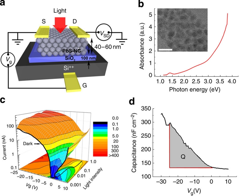
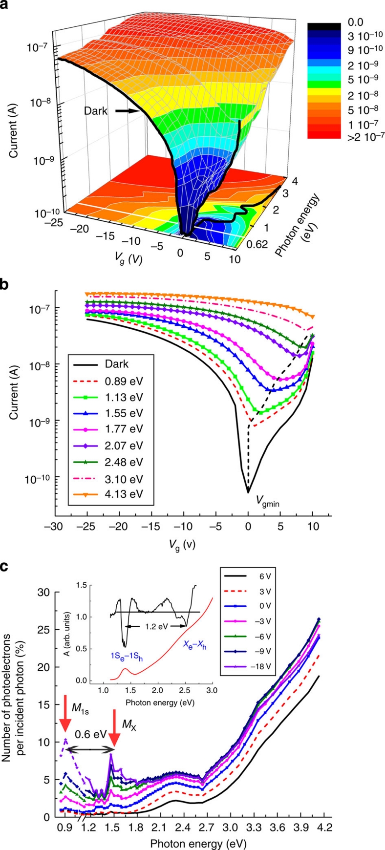
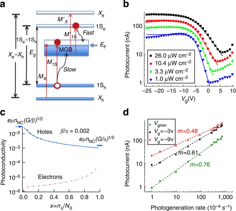
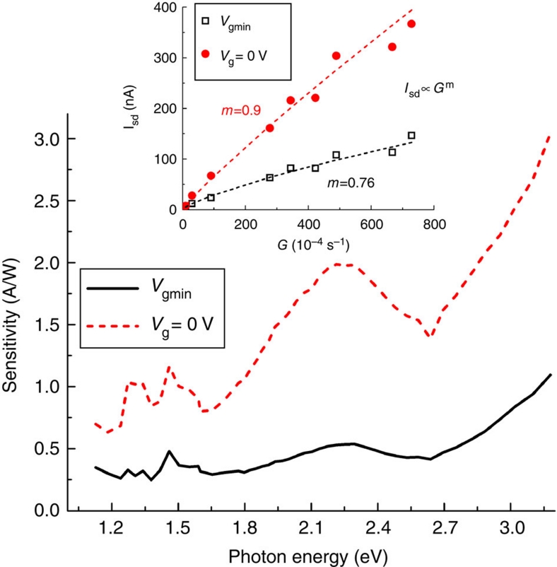
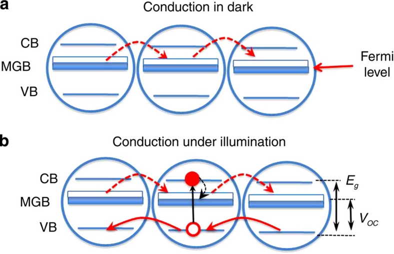
Colloidal semiconductor nanocrystals have attracted significant interest for applications in solution-processable devices such as light-emitting diodes and solar cells. However, a poor understanding of charge transport in nanocrystal assemblies, specifically the relation between electrical conductance in dark and under light illumination, hinders their technological applicability. Here we simultaneously address the issues of 'dark' transport and photoconductivity in films of PbS nanocrystals, by incorporating them into optical field-effect transistors in which the channel conductance is controlled by both gate voltage and incident radiation. Spectrally resolved photoresponses of these devices reveal a weakly conductive mid-gap band that is responsible for charge transport in dark. The mechanism for conductance, however, changes under illumination when it becomes dominated by band-edge quantized states. In this case, the mid-gap band still has an important role as its occupancy (tuned by the gate voltage) controls the dynamics of band-edge charges.


Figures

Figure 1
Figure 1. Dark conductance and photoconductance in PbS NC OFETs.
(a) A schematic of PbS–NC OFETs. S, D and G denote source, drain and gate electrodes, respectively. Illumination of PbS–NC films results in photoinduced current between the source and the drain electrodes, which is monitored as a function of light intensity and energy of incident photon, while simultaneously varying the gate voltage. (b) Absorption spectrum of PbS NCs in solution. The band-edge 1S peak is at 1.3 eV. The inset shows a representative transmission electron micrograph of the NCs (scale bar represents 10 nm). The mean NC diameter is 3.3±0.6 nm. (c) The Isd versus Vg characteristic in dark (black curve) and under 2.25 eV illumination as a function of light intensity (relative units; 1 corresponds to 30 μW cm−2) in a three-dimensional representation. Light illumination results in increased carrier concentration and a resultant orders-of-magnitude increase in photocurrent at the flat-band gate voltage (Vg=Vgmin; corresponds to the photocurrent minimum) due to the photoconductive effect. Under illumination, an extra positive voltage, which compensates for the photovoltage due to charge accumulation under the source/drain electrode, is required to achieve the flat-band condition (traced by the black line in the contour plot at the bottom). (d) Capacitance measurements for the NC film in dark indicate accumulation of holes in the channel under negative gate bias. The magnitude of the accumulated charge can be inferred from the integral formula image.
Figure 2
Figure 2. Spectrally resolved responses of OFET indicate presence of mid-gap states forming weakly conductive band.
(a) Isd-versus-Vg characteristics obtained in dark (black line) and under illumination as a function of photon energy starting from 0.62 eV (white line in the contour plot at the bottom). Coloured filling below the white line is interpolation between the measurements in dark and under 0.62 eV illumination. Black line in the contour plot at the bottom traces changes in the flat-band potential. (b) 'Cross-sections' obtained from the three-dimensional plots in panel 'a' show the variation of the source–drain current as a function of gate voltage under illumination at different photon energies (shown in the legend). (c) Photocurrent as a function of incident photon energy shown in terms of the number of photoelectrons per 100 incident photons (derived from data in panel 'a'). The spacing between the two prominent features (M1S and MX), that develop under negative bias, is half of the spacing between the 1S and X features in the second-derivative of the absorption (A) spectrum (inset). This suggests that the M1S and the MX peaks are likely due to transitions between the occupied 1S and X valence band states and the unoccupied MGB states, respectively.
Figure 3
Figure 3. Effect of MGB occupancy on photoconduction.
(a) The energy level diagram illustrating optical transitions between the NC-quantized and MGB states (red arrows) as well as relaxation pathways (wavy black arrows) for photogenerated band-edge carriers. The blue arrow marks the position of the Fermi level (EF). (b) Photocurrent measured at different gate voltages (symbols) for light intensities from 1.04 to 26.1 μW cm−2 (indicated in the figure legend) using 2.25 eV illumination. Lines are calculations using equations (4) and (5). In the modelling, the excitation intensity was characterized by the dimensionless quantity g=G/(βN02). On the basis of the photocurrent measured at large negative Vg for 26.1 μW cm−2 (solid black squares), g was determined to be 1.3×10⁻³. For other traces, g was obtained by scaling this value according to light intensity used in the measurements. γ and V0 were adjustable parameters determined from the fits. The obtained values systematically varied from 0.016 to 0.007 (±0.001) for γ and from 2 to 6 V (±0.15 V) for V0 with increasing light intensity. (c) Calculated photoconductivity due to electrons (dashed-and-doted red line) and holes (dashed black line) using equation (3) and assuming that x is within the interval from 0.05 to 0.95. Solid blue line is the hole photoconductivity obtained using equation (4). The arrows mark the hole-only (left) and electron-only (right) photoconductivities in the limits of x=0 and x=1, respectively. (d) The dependence of Isd on photogeneration rate for different gate voltages (3.1 eV photon energy). As expected for a transition from bimolecular to linear recombination, the log–log slope of this dependence is ~0.5 for the large negative gate bias (MGB is completely empty) and approaches unity as the gate bias gets more positive (MGB becomes populated).
Figure 4
Figure 4. Effect of gate bias on OFET sensitivity.
Sensitivity (defined as photocurrent per unity incident light intensity) as a function of photon energy at the flat-band voltage (solid black curve; purely photoconductive response) and Vg=0 (dashed red curve); 3.1 eV photon energy. The higher sensitivity in the latter case is a result of a combined contribution from the photoconductive and the photovoltaic effects. The contribution from the photovoltaic effect also increases the steepness of the dependence of the photocurrent on photogeneration rate (compare data shown by red solid circles and black open squares in the inset).
Figure 5
Figure 5. Conduction mechanisms in NC films in dark and under illumination.
(a) 'Dark' charge transport occurs through a manifold of weakly conductive MGB states. In our films, the MGB is completely full, and hence, insulating under the flat-band condition. Application of a negative gate bias leads to injection of holes into the MGB, which lowers the Fermi level and opens a conducting pathway through the MGB states. (b) The mechanism for charge transport changes under illumination. In this case, the photogenerated electrons get rapidly trapped from the conduction-band (CB) levels into the mid-gap states and are transported through the MGB. On the other hand, photogenerated holes, that are much longer lived, are transported via more-overlapping, highly conductive valence-band (VB) states. Hole transport via the VB levels dominates photoconduction. Because of the 'mixed' character of photoconduction, which involves both the VB and MGB states, the photovoltage is determined not by the intrinsic band-gap energy, Eg, but the VB–MGB separation.

References

    1. Murray C. B., Norris D. J. & Bawendi M. G. Synthesis and characterization of nearly monodisperse CdE (E=S, Se, Te) semiconductor nanocrystallites. J. Am. Chem. Soc. 115, 8706–8715 (1993).
    1. Mangolini L., Thimsen E. & Kortshagen U. High-yield plasma synthesis of luminescent silicon nanocrystals. Nano Lett. 5, 655–659 (2005). - PubMed
    1. Coe S., Woo W. K., Bawendi M. & Bulovic V. Electroluminescence from single monolayers of nanocrystals in molecular organic devices. Nature 420, 800–803 (2002). - PubMed
    1. Mueller A. H. et al.. Multicolor light-emitting diodes based on semiconductor nanocrystals encapsulated in GaN charge injection layers. Nano Lett. 5, 1039–1044 (2005). - PubMed
    1. Cho K. S. et al.. High-performance crosslinked colloidal quantum-dot light-emitting diodes. Nat. Photon. 3, 341–345 (2009).