. 2011 Oct 11;108(41):16900-5.
doi: 10.1073/pnas.1105113108. Epub 2011 Sep 29.

Large area and structured epitaxial graphene produced by confinement controlled sublimation of silicon carbide

Affiliations

Large area and structured epitaxial graphene produced by confinement controlled sublimation of silicon carbide

Walt A de Heer et al. Proc Natl Acad Sci U S A. .

Abstract

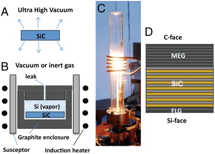
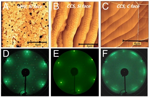
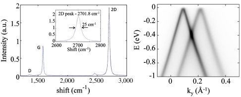
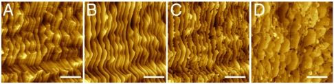
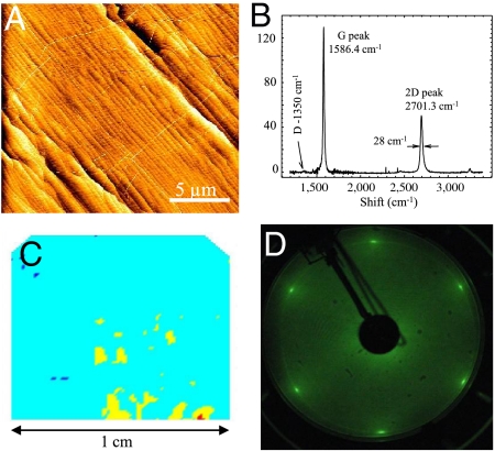
After the pioneering investigations into graphene-based electronics at Georgia Tech, great strides have been made developing epitaxial graphene on silicon carbide (EG) as a new electronic material. EG has not only demonstrated its potential for large scale applications, it also has become an important material for fundamental two-dimensional electron gas physics. It was long known that graphene mono and multilayers grow on SiC crystals at high temperatures in ultrahigh vacuum. At these temperatures, silicon sublimes from the surface and the carbon rich surface layer transforms to graphene. However the quality of the graphene produced in ultrahigh vacuum is poor due to the high sublimation rates at relatively low temperatures. The Georgia Tech team developed growth methods involving encapsulating the SiC crystals in graphite enclosures, thereby sequestering the evaporated silicon and bringing growth process closer to equilibrium. In this confinement controlled sublimation (CCS) process, very high-quality graphene is grown on both polar faces of the SiC crystals. Since 2003, over 50 publications used CCS grown graphene, where it is known as the "furnace grown" graphene. Graphene multilayers grown on the carbon-terminated face of SiC, using the CCS method, were shown to consist of decoupled high mobility graphene layers. The CCS method is now applied on structured silicon carbide surfaces to produce high mobility nano-patterned graphene structures thereby demonstrating that EG is a viable contender for next-generation electronics. Here we present for the first time the CCS method that outperforms other epitaxial graphene production methods.


Conflict of interest statement

The authors declare no conflict of interest.

Figures

Fig. 1.
Fig. 1.
The confinement controlled sublimation method. (A) SiC wafer in UHV: Sublimed silicon is not confined, causing rapid, out of equilibrium graphene growth. (B) The CCS method: sublimed Si gas is confined in a graphite enclosure so that growth occurs in near thermodynamic equilibrium. Growth rate is controlled by the enclosure aperture (leak), and the background gas pressure. (C) Photograph of the induction furnace. (D) Under CCS conditions few layer graphite (FLG, from 1 to 10 layers) grows on the Si terminated face, and multilayer epitaxial graphene (MEG, from 1 to 100 layers) grows on the C terminated face.
Fig. 2.
Fig. 2.
Comparison of UHV and CCS grown epitaxial graphene. (AC) AFM images and (DF) LEED patterns. (A) UHV grown monolayer on the Si-face. (B) CCS monolayer grown on Si-face. (C) MEG on C-face; note that layers drape over the substrate steps (white lines are pleats in the MEG layer). (D) LEED pattern of CCS grown Si-face graphene monolayer (bright spots due to graphene) showing typical surface reconstruction features. (E) LEED image of CCS grown C-face monolayer; (F) LEED image of CCS grown C-face multilayer (MEG), showing characteristic “arcs” due to the rotational stacking.
Fig. 3.
Fig. 3.
Raman (Left) and ARPES (Right) spectroscopy of MEG. Raman spectrum shows the characteristic G and 2D graphene peaks. The 2D peak of this approximately 100 layer MEG sample fits a single Lorentzian of full width 25 cm-1, centered at 2701.8 cm-1. A weak D peak can be discerned. ARPES data from the top three layers of a 10-layer sample around ky = 0 (i.e., the Dirac point). Two unperturbed cones are observed showing that the layers are electronically decoupled: The slope is vF = 1 × 106 m/s, as expected for isolated graphene, and the Fermi level is with 20 meV from the Dirac point. For details, see ref. .
Fig. 4.
Fig. 4.
AFM images showing the evolution of the surface of the 6H Si-face upon annealing. (A) initial surface after hydrogen etching showing half-unit cell steps (0.8 nm) resulting from the miscut; (B) After CCS annealing at 1,300 °C: substrate steps become rounded, (C) annealing at 1,400 °C; the steps roughen, and (D) 1,500 °C: formation of a graphene layer. The scale bar is 5 μm.
Fig. 5.
Fig. 5.
Single layer graphene grown on a 1 cm × 1 cm 4H-SiC chip on the C-face. (A) AFM image showing a graphene coated stepped SiC surface; note the continuous pleats running across large regions of the surface. (B) The Raman spectrum (after SiC background subtraction); the 2D peak consists of single Lorentzian (full width = 28 cm-1); the disorder induced D peak is absent. (C) Ellipsometry shows graphene uniformity (color scale light blue: 1 layer, yellow: 2 layers, red: 3 layers, dark blue: no graphene; beam size: 250 μm × 250 μm). (D) LEED pattern of the monolayer.
Fig. 6.
Fig. 6.
Examples of template grown graphene structures etched on the (0001) face. (A) 4H-SiC hydrogen-etched surface with a regular step structure. (B) Flat step-free graphitized mesa with MEG pleats (C) circular mesa etched on Si-face; the hexagonal shape results from the annealing at 1,550 °C showing preference for the (1–10 n) crystal surfaces (n depends on the step height and ranges from 2 for nm steps to about 10 for μm steps). (D) Electrostatic force microscopy image after CCS annealing; graphene (light) grows on the mesa sidewalls but not on the horizontal (0001) surfaces.
Fig. 7.
Fig. 7.
Patterned sidewall ribbons. (A) and (B) are AFM images of 10 nm deep trenches etched at right angles and graphitized. Trench width is 100 nm with a 300 nm pitch. (C) An ARPES image of the Dirac cone from graphene grown only on the sidewalls. (D) A cross-section of the trenches in B after graphitization. (E) Two height profiles along the top of the trenches in B showing a small rms height variation.

References

    1. Boehm H, Clauss A, Hofmann U, Fischer G. Dunnste Kohlenstof-Folien. Z Naturforsch Pt B. 1962;17:150–153.
    1. Van Bommel A, Crombeen J, van Tooren A. LEED and Auger-electron observations of SiC (0001) surface. Surf Sci. 1975;48:463–472.
    1. Gall NR, RutKov EV, Tontegode AY. Two dimensional graphite films on metals and their intercalation. Int J Mod Phys B. 1997;11:1865–1911.
    1. de Heer WA, Berger C, First PN. 7015142. US Patent. 2006
    1. de Heer WA. Early Development of Graphene Electronics. 2009. Available at http://hdl.handle.net/1853/31270.

LinkOut - more resources