. 2011:2:85-98.
doi: 10.3762/bjnano.2.10. Epub 2011 Feb 4.

Manipulation of gold colloidal nanoparticles with atomic force microscopy in dynamic mode: influence of particle-substrate chemistry and morphology, and of operating conditions

Affiliations

Manipulation of gold colloidal nanoparticles with atomic force microscopy in dynamic mode: influence of particle-substrate chemistry and morphology, and of operating conditions

Samer Darwich et al. Beilstein J Nanotechnol. 2011.

Abstract

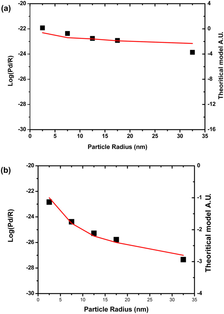
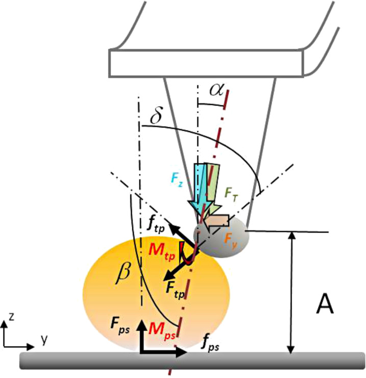
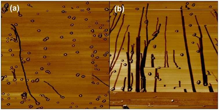
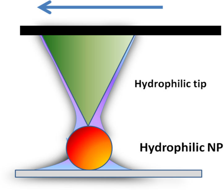
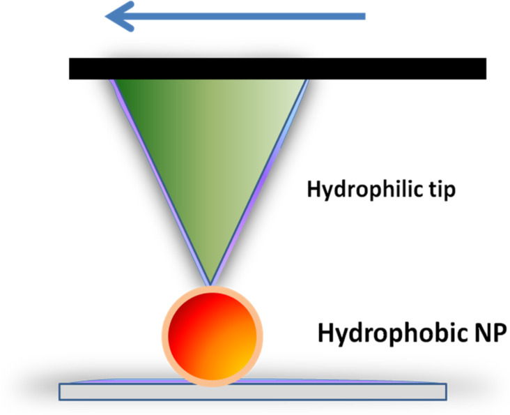
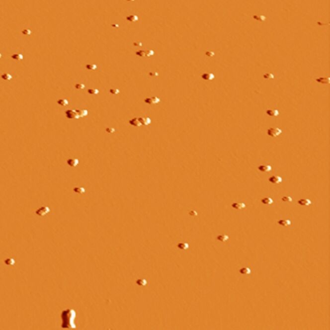
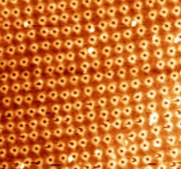
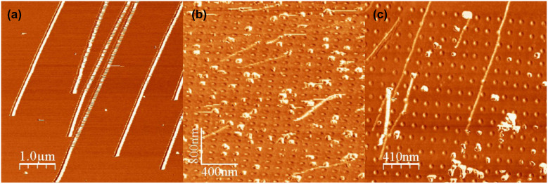
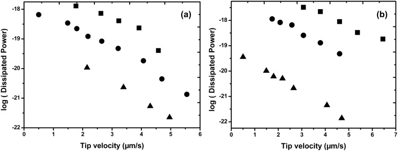
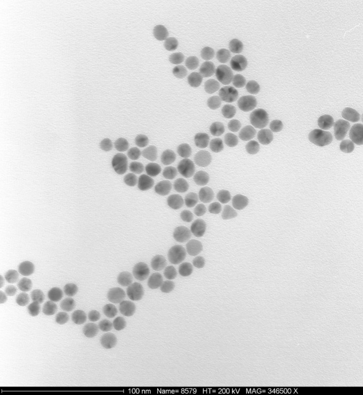
One key component in the assembly of nanoparticles is their precise positioning to enable the creation of new complex nano-objects. Controlling the nanoscale interactions is crucial for the prediction and understanding of the behaviour of nanoparticles (NPs) during their assembly. In the present work, we have manipulated bare and functionalized gold nanoparticles on flat and patterned silicon and silicon coated substrates with dynamic atomic force microscopy (AFM). Under ambient conditions, the particles adhere to silicon until a critical drive amplitude is reached by oscillations of the probing tip. Beyond that threshold, the particles start to follow different directions, depending on their geometry, size and adhesion to the substrate. Higher and respectively, lower mobility was observed when the gold particles were coated with methyl (-CH(3)) and hydroxyl (-OH) terminated thiol groups. This major result suggests that the adhesion of the particles to the substrate is strongly reduced by the presence of hydrophobic interfaces. The influence of critical parameters on the manipulation was investigated and discussed viz. the shape, size and grafting of the NPs, as well as the surface chemistry and the patterning of the substrate, and finally the operating conditions (temperature, humidity and scan velocity). Whereas the operating conditions and substrate structure are shown to have a strong effect on the mobility of the particles, we did not find any differences when manipulating ordered vs random distributed particles.

Keywords: atomic force microscopy; intermolecular interaction; manipulation; nanoparticles; precise positioning; self-assembled monolayers.


Figures

Figure 1
Figure 1
Evolution of the logarithm of the dissipated power normalized by the radius (R) as a function of (a) as-synthesized spherical Au nanoparticles on bare silicon wafer versus the particle radius R (squares: experimental data; solid line: theoretical data) corresponding to a pure sliding model and (b) spherical Au nanoparticles on silicon wafer coated with –CH3 terminated groups (hydrophobic coating) versus the particle radius R (squares: experimental data, solid line: theoretical data) corresponding to a pure rotation model. Both after the tap of a tip in a typical AFM tapping mode manipulation as described by Sitti [–38].
Scheme 1
Scheme 1
Scheme presenting the different forces during tip–particle and particle–substrate interactions, and the angles α, β and δ.
Figure 2
Figure 2
Typical trajectories of bare gold nanoparticles (20 nm diameter) on a silicon substrate when the probing tip moves along a zigzag path: (a) low drive amplitude, (b) high drive amplitude. Scan size: 5 µm.
Figure 3
Figure 3
Typical scan patterns used in AFM: (a) raster scan path used by Nanosurf (b) zigzag scan path used by Veeco. Top view: the grey disk corresponds to the position of the tip on the surface and the yellow, blue and red disks are the positions of spherical particles pushed by the tip along its scan path.
Figure 4
Figure 4
AFM images of nanocluster movement during their manipulation (a) gold nanorods deposited onto silicon wafer, scan size: 12 µm; (b) antimony islands on HOPG, scan size: 1.5 µm; (c) Au nanotriangles on silicon wafer. Middle triangles have been intentionally colored in to illustrate the trajectory of the Au nanoparticles during manipulation, scan size: 5 µm.
Figure 5
Figure 5
(a) Average power dissipation accompanying the onset of motion of as-synthesized and coated nanoparticles on silicon in air vs temperature. Black columns: as-synthesized NPs that are uniformly distributed on the substrate, dark gray columns: CH3-coated NPs, light gray columns: as-synthesized NPs randomly distributed on the substrate. (b) Logarithm of the dissipated power in moving as-synthesized and coated NPs on silicon wafer vs reciprocal temperature. Closed squares: as-synthesized nanoparticules, open circles: as-synthesized nanoparticles ordered organized, open squares: CH3-coated nanoaprticles, closed triangles: OH-coated nanoparticles.
Figure 6
Figure 6
AFM images of 25 nm diameter gold nanoparticles deposited onto a silicon wafer. (a) Ordered organization as described in the Experimental section, (b) random distribution. Frame sizes: 3 µm and 1 µm, respectively.
Scheme 2
Scheme 2
Formation of two capillary water bridges between hydrophilic tip and particle, and particle and surface.
Scheme 3
Scheme 3
Formation of two water layer films between hydrophilic tip–hydrophobic particle, and hydrophobic particle–hydrophilic surface, respectively.
Figure 7
Figure 7
As-synthesized Au particles on silicon in ultra-high vacuum. Frame size: 3 µm.
Figure 8
Figure 8
AFM image of nanopatterned surface exhibiting Si pits: Frame size: 3 µm.
Figure 9
Figure 9
Manipulation of as-synthesized Au nanoparticles on (a) a flat silicon wafer with a spacing of 9.7 nm and (b) a nanopatterned one with a spacing 16 nm, and (c) a patterned wafer with a spacing of 3.9 nm.
Figure 10
Figure 10
Logarithm of the dissipated power in moving as-synthesized NPs on silicon wafer versus the tip scan speed. Substrates: circles: SiO2 silicon wafer; squares: NH2-coated silicon wafer (hydrophilic substrate); triangles: CH3-coated silicon wafer (hydrophobic substrate). (a) 35 nm diameter Au NPs, (b) 60 nm diameter Au NPs.
Figure 11
Figure 11
400 nm × 400 nm TEM image of 25 nm diameter gold nanoparticles.

References

    1. Kottas G S, Clarke L I, Horinek D, Michl J. Chem Rev. 2005;105:1281. doi: 10.1021/cr0300993. - DOI - PubMed
    1. Storhoff J J, Marla S S, Bao P, Hagenow S, Mehta H, Lucas A, Garimella V, Patno T, Buckingham W, Cork W, et al. Biosens Bioelectron. 2004;19:875. doi: 10.1016/j.bios.2003.08.014. - DOI - PubMed
    1. Schaefer D, Reifenberger R, Patil A, Andres R P. Appl Phys Lett. 1995;66:1012. doi: 10.1063/1.113589. - DOI
    1. Yamamoto Y, Kurosawa O, Kabata H, Shimamoto N, Washizu M. Molecular surgery of DNA based on electrostatic micromanipulation. Thirty-Third IAS Annual Meeting, 1998; The 1998 IEEE Industry Applications Conference; 1998 Oct 12-15; St. Louis, MO, USA. 1998. p. 1933. - DOI
    1. Vonna L, Wiedemann A, Aepfelbacher M, Sackmann E. J Cell Sci. 2003;116:785. doi: 10.1242/jcs.00230. - DOI - PubMed

LinkOut - more resources