. 2011 Nov 9;479(7372):203-7.
doi: 10.1038/nature10569.

Two types of luminescence blinking revealed by spectroelectrochemistry of single quantum dots

Affiliations

Two types of luminescence blinking revealed by spectroelectrochemistry of single quantum dots

Christophe Galland et al. Nature. .

Abstract

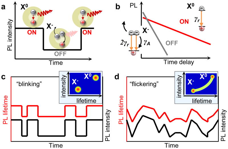
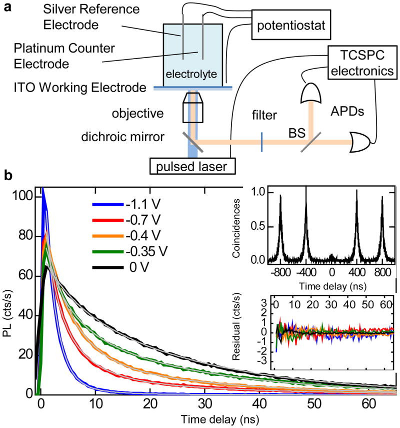
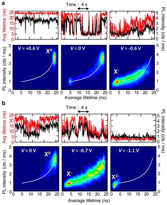
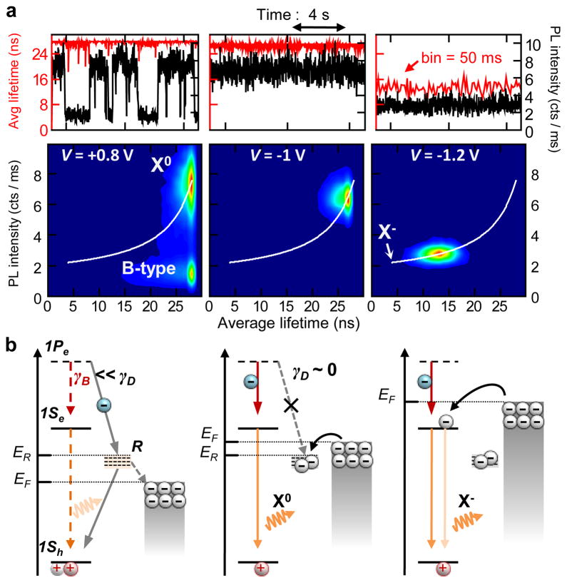
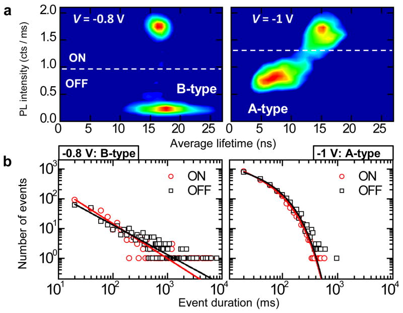
Photoluminescence blinking--random switching between states of high (ON) and low (OFF) emissivities--is a universal property of molecular emitters found in dyes, polymers, biological molecules and artificial nanostructures such as nanocrystal quantum dots, carbon nanotubes and nanowires. For the past 15 years, colloidal nanocrystals have been used as a model system to study this phenomenon. The occurrence of OFF periods in nanocrystal emission has been commonly attributed to the presence of an additional charge, which leads to photoluminescence quenching by non-radiative recombination (the Auger mechanism). However, this 'charging' model was recently challenged in several reports. Here we report time-resolved photoluminescence studies of individual nanocrystal quantum dots performed while electrochemically controlling the degree of their charging, with the goal of clarifying the role of charging in blinking. We find that two distinct types of blinking are possible: conventional (A-type) blinking due to charging and discharging of the nanocrystal core, in which lower photoluminescence intensities correlate with shorter photoluminescence lifetimes; and a second sort (B-type), in which large changes in the emission intensity are not accompanied by significant changes in emission dynamics. We attribute B-type blinking to charge fluctuations in the electron-accepting surface sites. When unoccupied, these sites intercept 'hot' electrons before they relax into emitting core states. Both blinking mechanisms can be electrochemically controlled and completely suppressed by application of an appropriate potential.


Figures

Figure 1
Figure 1. Conventional charging model: A-type blinking and flickering
a, In the conventional PL blinking model, ON and OFF periods correspond to a neutral (X0) and a charged (X) nanocrystal, respectively. b, Schematic PL decay of the ON and the OFF states on a logarithmic scale. The dynamics of the ON state is dominated by the radiative rate γr. In the charged state, the increase in the number of recombination pathways leads to a faster radiative rate (2γr) responsible for the higher emission intensity at short delays. Simultaneously, the onset of three-particle Auger recombination with the rate γAγr opens a new nonradiative channel, leading to faster PL decay and reduced PL QY. c, When the time-scale of charging/discharging is longer than the experimental binning time, binary blinking is observed. d, For fluctuations much faster than the bin size, a continuous distribution of intensities and lifetimes is obtained, often referred to as “flickering”. The insets in (c) and (d) show schematically the corresponding Fluorescence Intensity – Lifetime Distributions (FLIDs).
Figure 2
Figure 2. Experimental setup and electrochemical charging of an individual nanocrystal
a, Schematics of a single-nanocrystal spectroelectrochemical experiment. b, Series of PL decays for a single nanocrystal under increasing negative potential. The thin grey lines show the best global tri-exponential fit with the shared time constants, yielding the lifetimes τs = 2 ns, τm = 5 ns, and τl = 24 ns. Insets: The second-order PL intensity correlation function (top) measured for this nanocrystal indicates g2(0) = 0.08. Residuals of the global fit (bottom) indicate very high fidelity of the fitting procedure with deviations within the noise level and below 1% of the maximum PL signal.
Figure 3
Figure 3. Correlated PL intensity and lifetime fluctuations: A-type blinking and flickering
a, PL intensity (black lines) and average lifetime (red lines) trajectories and corresponding FLIDs for the nanocrystal shown in Figs. 2b–c at three different potentials. Binary blinking seen at V = 0 V is suppressed at V = +0.6 V, whereas electron injection is achieved at V = −0.6 V. In the FLID color scale, red corresponds to the most frequently occurring intensity-lifetime pair, while probabilities below 1% of this maximum are represented by dark blue. A linear scaling from blue to red is used in-between. b, Data from the same nanocrystal, acquired on a different day, display continuous PL intensity and lifetime fluctuations, typical of flickering. At V = −1.1 V, we observe emission from a doubly charged exciton X2−. All data were analyzed with a bin size of 50 ms. Full time trajectories for (a) and (b) are shown in Supplementary Fig. 1.
Figure 4
Figure 4. PL intensity fluctuations without lifetime changes: B-type blinking
a, PL intensity (black lines) and average lifetime (red lines) trajectories and corresponding FLIDs for a nanocrystal showing the B-type OFF state (labeled ‘D’ in FLID); analysis with a 10 ms bin. Full time trajectories are shown in Supplementary Fig. 6. b, The model of B-type blinking. The B-type OFF state is due to the activation of recombination centers (‘R’) that capture hot electrons with the rate γD which is faster than the intraband relaxation rate γB (the ground and the excited electron states are shown as 1Se and 1Pe, respectively). The position of the Fermi level (EF) relative to the trap energy (ER) is determined by the electrochemical potential and controls the occupancy of the surface trap R. This, in turn, allows for electrochemical control of B-type blinking.
Figure 5
Figure 5. Electrochemically controlled switching between two distinct ON/OFF times statistics in the same nanocrystal accompanying the transition from B- to A-type blinking
a, FLIDs indicating a nanocrystal switching from B-type at −0.8 V (left) to A-type blinking at −1 V (right). Details of the analysis are given in Supplementary Fig. 9. b, ON (red circles) and OFF (black squares) event duration statistics for the FLIDs in ‘a’ in the log-log representation. At −0.8 V, we fit the data to a power-law distribution, ∝tα, with α = 1.17 for the ON times (red line) and α = 1.00 for the OFF times. At −1 V, in the A-type blinking mode, the power-law breaks down. The data, however, can be closely fitted by introducing an exponential cut-off in the form: tαexp(−t/tc), where α = 0.54, tc = 73.4 ms for the ON times (red line) and α = 0.37, tc = 70.8 ms for the ON times (black line).

References

    1. Hoogenboom JP, Hernando J, van Dijk EMHP, van Hulst NF, García-Parajó MF. Power-law blinking in the fluorescence of single organic molecules. ChemPhysChem. 2007;8:823–833. - PubMed
    1. Bout DAV, et al. Discrete intensity jumps and intramolecular electronic energy transfer in the spectroscopy of single conjugated polymer molecules. Science. 1997;277:1074–1077.
    1. Riley EA, Bingham C, Bott ED, Kahr B, Reid PJ. Two mechanisms for fluorescence intermittency of single violamine R molecules. Phys Chem Chem Phys. 2011;13:1879–1887. - PubMed
    1. Frantsuzov P, Kuno M, Janko B, Marcus RA. Universal emission intermittency in quantum dots, nanorods and nanowires. Nat Phys. 2008;4:519–522.
    1. Nirmal M, et al. Fluorescence intermittency in single cadmium selenide nanocrystals. Nature. 1996;383:802–804.

Publication types