. 2011:2.
doi: 10.3402/nano.v2i0.5883. Epub 2011 Feb 16.

Anisotropic nanomaterials: structure, growth, assembly, and functions

Affiliations

Anisotropic nanomaterials: structure, growth, assembly, and functions

Panikkanvalappil R Sajanlal et al. Nano Rev. 2011.

Abstract

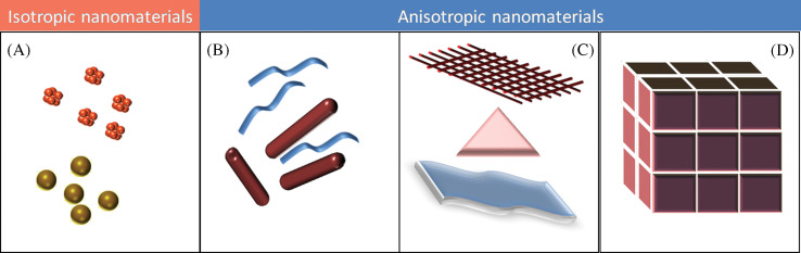
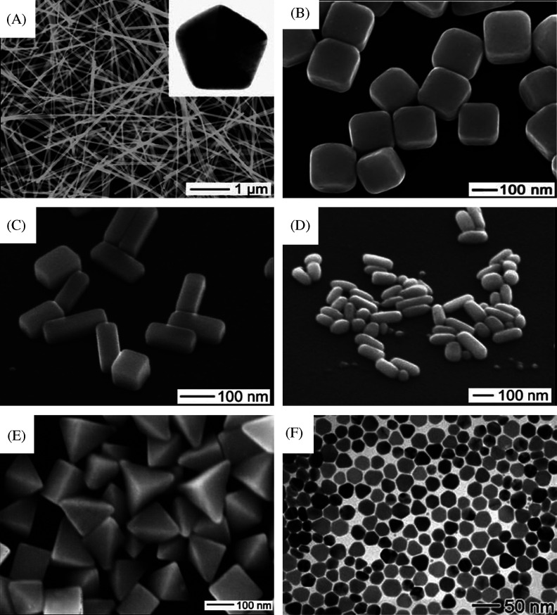
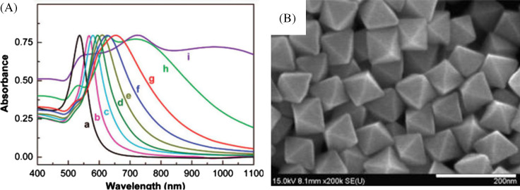
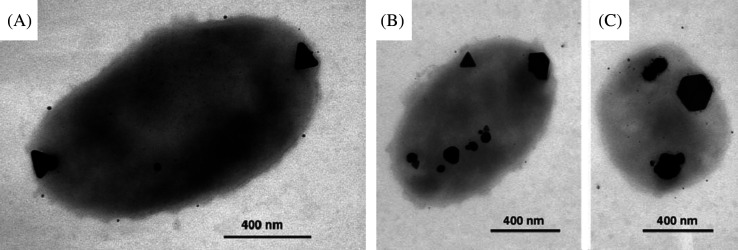
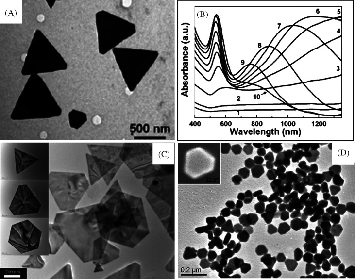
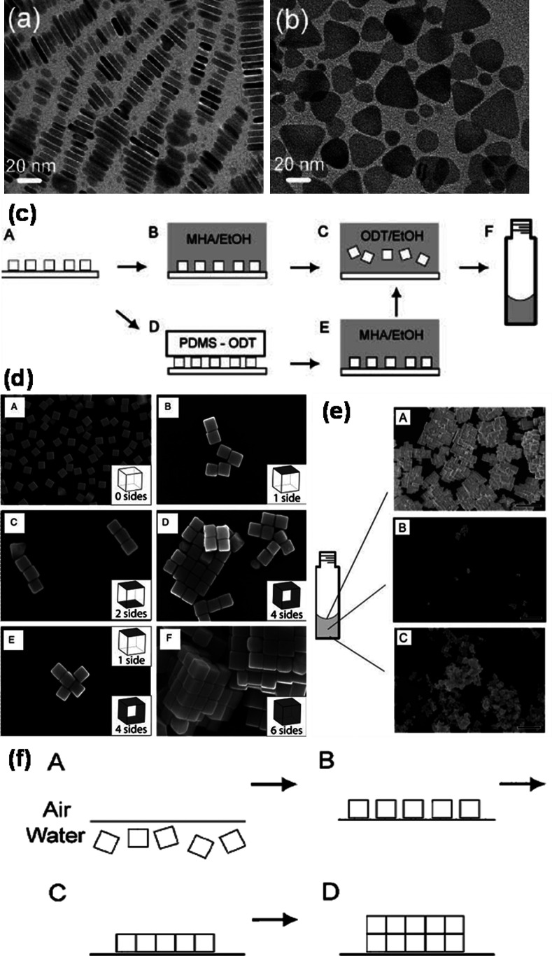
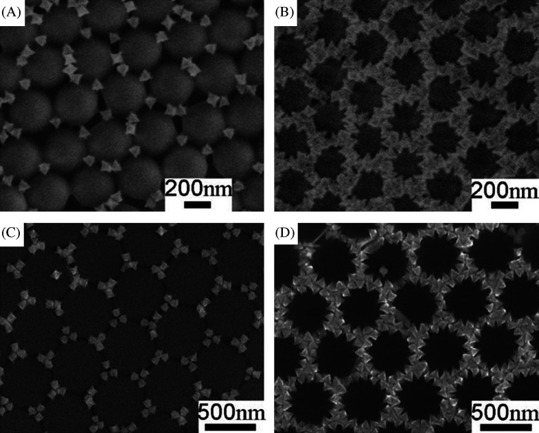
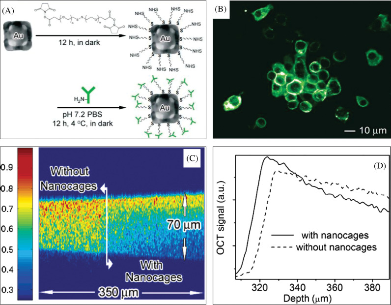
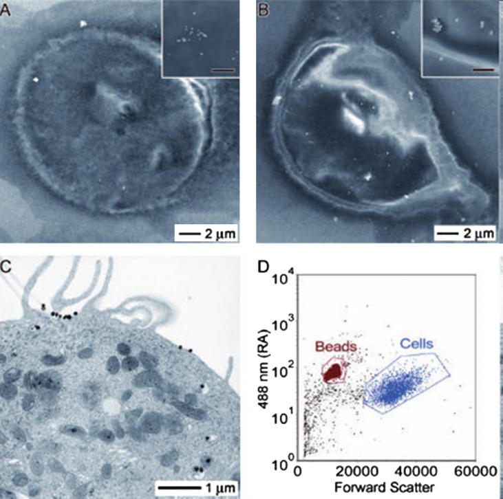
Comprehensive knowledge over the shape of nanomaterials is a critical factor in designing devices with desired functions. Due to this reason, systematic efforts have been made to synthesize materials of diverse shape in the nanoscale regime. Anisotropic nanomaterials are a class of materials in which their properties are direction-dependent and more than one structural parameter is needed to describe them. Their unique and fine-tuned physical and chemical properties make them ideal candidates for devising new applications. In addition, the assembly of ordered one-dimensional (1D), two-dimensional (2D), and three-dimensional (3D) arrays of anisotropic nanoparticles brings novel properties into the resulting system, which would be entirely different from the properties of individual nanoparticles. This review presents an overview of current research in the area of anisotropic nanomaterials in general and noble metal nanoparticles in particular. We begin with an introduction to the advancements in this area followed by general aspects of the growth of anisotropic nanoparticles. Then we describe several important synthetic protocols for making anisotropic nanomaterials, followed by a summary of their assemblies, and conclude with major applications.


Figures

Fig. 1
Fig. 1
Various kinds of nanomaterials. (A) 0D spheres and clusters. (B) 1D nanofibers, wires, and rods. (C) 2D films, plates, and networks. (D) 3D nanomaterials.
Fig. 2
Fig. 2
Number of papers published during the last decade (1998–2009), including certain keywords (as indicated) in their title. Source: ISI Web of Science.
Fig. 3
Fig. 3
(A) TEM image of Au triangular nanoparticles. The inset is the SAED pattern taken from individual nanoprism. (B) UV-vis-NIR spectra of purified Au nanoprisms (blue trace) and DDA calculation (red trace). Reproduced with permission from Reference (23). American Chemical Society, Copyright (2005).
Fig. 4
Fig. 4
(A) TEM image of Au@Pd nanocubes. (B) TEM image of a single Au@Pd nanocube at high magnification. The inset is the SAED pattern taken from individual nanocube. (C) STEM images of the octahedral Au seed within a cubic Pd shell and cross-sectional compositional line profiles of a Au@Pd nanocube along the diagonal (indicated by a red line). D and E are TEM images of Au@Ag nanocubes and Au@Pt nanoparticles, respectively. Reproduced with permission from Reference (166). American Chemical Society, Copyright (2008).
Fig. 5
Fig. 5
Table shows the shapes of gold particles and corresponding reaction conditions. A–D are the TEM images of various anisotropic Au nanoparticles synthesized under different conditions. Inset of C shows the corresponding SEM image. Scale bars are (100 nm). Reproduced with permission from Reference (168). American Chemical Society, Copyright (2004).
Fig. 6
Fig. 6
A and B are SEM and TEM images of star-shaped gold nanocrystals, respectively. Inset of B shows the SAED pattern taken from a single nanostar. An extinction spectrum of the nanostar solution exhibits broad visible and NIR peaks (C). Reproduced with permission from Reference (39). American Chemical Society, Copyright (2006).
Fig. 7
Fig. 7
TEM image of Au nanostars synthesized through reduction of HAuCl4 in a PVP/DMF mixture, in the presence of preformed Au seeds, using 10 mM PVP. Reproduced with permission from Reference (42). Institute of Physics, Copyright (2006).
Fig. 8
Fig. 8
Large area (A) and corresponding single particle. (B) Field-emission scanning electron microscopy (FESEM) images of gold MFs. (C) An enlarged FESEM image of a single stem of the MF showing ridges along the edges. (D) Top view of a single stem of the MF showing the pentagonal structure. Reproduced with permission from Reference (169). Springer, Copyright (2009).
Fig. 9
Fig. 9
Cartoon representation of (A) 3-D morphology showing (111) end-faces and (100) side-faces. (B) Illustration of ‘zipping’ mechanism for the formation of the bilayer of CTAB (squiggles) on the NR (black rectangle) surface may assist NR formation as more gold ion (black dots) is introduced. Reproduced with permission from Reference (170). American Chemical Society, Copyright (2005 and 2003).
Fig. 10
Fig. 10
HRTEM images of NRs formed using different seed particles: (A) Fe (bcc), (B) Cd (hcp), (C) Sb (trigonal), and (D) In (tetragonal). Although the metals are of different crystal structures, the GNRs formed are fcc. Reproduced with permission from Reference (173). Springer-Netherlands, Copyright (2010).
Fig. 11
Fig. 11
Absorption spectrum of GNRs. The arrows correspond to the electron motions.
Fig. 12
Fig. 12
A schematic illustrating various stages of the reaction that leads to the formation of noble-metal nanoparticles with different shapes. After the formation of nuclei (small clusters), they become seeds with a single-crystal, singly twinned, or multiply twinned structure. Stacking faults in the seeds results in plate-like structures. Green, orange, and purple represent the (100,111), and (110) facets, respectively. The parameter R is defined as the ratio between the growth rates along the (100) and (111) directions. Twin planes are delineated in the drawing with magenta lines. Reproduced with permission from Reference (178). Wiley-VCH, Copyright (2004).
Fig. 13
Fig. 13
(A) Large area SEM image of Ag NWs. Inset shows a cross-sectional TEM image of a microtomed NW, revealing its fivefold twinned crystal structure and pentagonal profile Reproduced with permission from Reference (179). American Chemical Society, Copyright (2008). (B) SEM image of Ag nanocubes. Reproduced with permission from Reference (180). American Association for the Advancement of Science (AAAS), Copyright (2002). (C) SEM image of the Ag nanobars produced when NaCl was substituted with NaBr (181). (D) SEM of nanorice at a 45° tilt. (E) SEM images of bipyramids approximately 75 and 150 nm in edge length (159). (F) SEM images of silver nanoplates prepared in the presence of PAM at 135°C for 3 h. Reproduced with permission from Reference (182). Royal Society of Chemistry, Copyright (2007).
Fig. 14
Fig. 14
UV-vis absorption spectra for Au octahedra with different edge lengths dispersed in water (A). The edge lengths of Au octahedra from curve ‘a’ to curve ‘i’ were 20, 50, 63, 80, 95, 110, 125, 160, and 230 nm, respectively. SEM images of Au octahedra with average edge lengths of 63 nm synthesized at 195°C by introducing 1 M HCl solution to the initial gold precursor. Scale bars: 200 nm. Reproduced with permission from Reference (184). American Chemical Society, Copyright (2008).
Fig. 15
Fig. 15
(A) TEM image of large, triangular, Ag-containing particles at both poles produced by P. stutzeri AG259. An accumulation of smaller Ag-containing particles can be found all over the cell. (B and C) Triangular, hexagonal, and spheroidal Ag-containing nanoparticles accumulated at different cellular binding sites. Reproduced with permission from Reference (186). Proceedings of National Academy of Science, Copyright (1999).
Fig. 16
Fig. 16
(A) TEM image of gold nanotriangle synthesized by the reduction of aqueous HAuCl4 solution with lemon grass extract. Reproduced with permission from Reference (189). American Chemical Society, Copyright (2005). (B) UV-vis-NIR spectra of gold nanoparticles synthesized by adding different amount of lemongrass leaf extract to 5 mL of 10−3 M HAuCl4 solution. Curves 1–10 correspond to solutions with 0.2, 0.3, 0.4, 0.5, 0.6, 0.7, 0.8, 1.0, 1.2, and 1.6 mL of lemongrass leaf extract in 5 mL of 10−3 M HAuCl4 solution, respectively. (C) TEM images of gold nanoplates synthesized by the reduction of aqueous AuCl4− by seaweed extract. Reproduced with permission from Reference (192). American Chemical Society, Copyright (2005). Single-crystalline Ag nanoplates synthesized in aqueous medium at room temperature using an extract of the unicellular green alga Chlorella vulgaris (Fig. 13D). Inset shows the SEM image of a single Ag nanoplate. Reproduced with permission from Reference (193). American Chemical Society, Copyright (2007).
Fig. 17
Fig. 17
SEM images showing (A) single-, (B) double-, and (C) triple-turn hexagonal ring-like superstructures of hexagonal single-crystals of Co-doped ZnO NRs. Reproduced with permission from Reference (201). American Chemical Society, Copyright (2008). D and E are SEM images of the Ag2V4O11 nanorings (f) SEM images of the Ag2V4O11 microloops formed by rolling of several nanobelts. Reproduced with permission from Reference (202). American Chemical Society, Copyright (2006).
Fig. 18
Fig. 18
(A) SEM image of the octahedral gold nanocrystals. The imaged regions show extensive self-assembled structures. (B) UV-vis absorption spectra of octahedral nanoparticles of different sizes. Maximum absorbance of the spectra has been normalized. Reproduced with permission from Reference (204). American Chemical Society Copyright (2008).
Fig. 19
Fig. 19
(A) Schematic of galvanic displacement reaction. (B) SEM image of Ag nanoplates formed on the surface of n-type (110) GaAs wafer. Reproduced with permission from Reference (208). American Chemical Society, Copyright (2007). (C) Silver nano-inukshuks prepared by immersing n-type Ge(100) in aqueous AgNO3 solution. Inset shows the close-up view of facets on the tips of silver metallic nano-inukshuks. Reproduced with permission from Reference (209). American Chemical Society, Copyright (2005). SEM images of silver (D) (Reproduced with permission from Reference (210). American Chemical Society, Copyright (2007)) and gold (E) (Reproduced with permission from Reference (211). Institute of Physics, Copyright (2006)) dendrites formed on zinc plates.
Fig. 20
Fig. 20
(A) SEM and TEM (inset) images of Au nanocages. Reproduced with permission from Reference (212). American Chemical Society Copyright (2004). (B) SEM image of the Au nanoframes. Reproduced with permission from Reference (213). Copyright (2008) Springer. C, E are SEM images, and D, F are TEM images of single-walled nanotube of Au/Ag alloy and double-walled nanotube of Au/Ag alloy, respectively. Reproduced with permission from Reference (216). Wiley, Copyright (2008).
Fig. 21
Fig. 21
The bimodal growth of Ag nanoprisms. (a) TEM image of a sample of Ag nanoprisms formed using single-beam excitation; inset, histograms used to characterize the size distribution as bimodal. B and C are the TEM images of nanoprism stacks showing that nanoprisms have nearly identical thicknesses. (d) Schematic diagram of the proposed light-induced fusion growth of Ag nanoprisms. Reproduced with permission from Reference (26). American Association for the Advancement of Science, Copyright (2001).
Scheme 1
Scheme 1
Electrochemical synthesis metal colloids
Fig. 22
Fig. 22
(A) Schematics of the electrochemical set-up used for the synthesis of gold nanocubes. (B) TEM images of gold nanocubes. Inset shows a SAED pattern taken from any individual nanocube by directing the electron beam perpendicular onto one of its square faces. (C) UV-vis absorption spectra of various gold nanoparticles obtained with different injection rates of acetone. Reproduced with permission from Reference (224). American Institute of Physics, Copyright (2008).
Fig. 23
Fig. 23
SEM images of platinum nanothorns. (a) Large area SEM image; (b) high magnification SEM image of a platinum nanothorn; (c) side view of a nanothorn; (c) top view of a nanothorn. The scale bar in (b), (c), and (d) is 100 nm. Reproduced with permission from Reference (226). Royal Society of Chemistry, Copyright (2006).
Fig. 24
Fig. 24
(A and B) FESEM images of an alumina membrane. (C) Schematic representation of the successive stages during formation of GNRs via the template method. (D) TEM micrographs of GNRs obtained by the template method. Reproduced with permission from Reference (234). American Chemical Society, Copyright (2000).
Fig. 25
Fig. 25
(A) Schematic of a single GNR. (B) HRTEM showing the different crystal planes and lattice structure. (C) Schematic showing the different ways of arranging the NRs.
Fig. 26
Fig. 26
Electron micrograph showing the border of the self-assemblies. The thickness increases from top to bottom. The inset shows a magnified part of an assembly. Scheme of the deposition method is also shown in the figure. Reproduced with permission from Reference (250). American Chemical Society, Copyright (2000).
Fig. 27
Fig. 27
TEM images of bundles of DNA-linked GNRs. (A) The three-strand (B) two-strand DNA linking systems. UV-vis spectra of (C) a suspension of non-complementary DNA functionalized NRs and (D) the two-strand NR system before (—) and after (····) duplexation at 25°C. Reproduced with permission from Reference (253). Royal Society of Chemistry, London, Copyright (2001).
Fig. 28
Fig. 28
(A) Schematic of the general mechanism of GNR nanochain formation due to electrostatic interaction due to cysteine and glutathione. Reprinted with permission from Reference (262). American Chemical Society, Copyright (2005).
Fig. 29
Fig. 29
TEM images taken in the (A) low MAG and (B) MAG I modes of the same area, showing self-assembly of NRs, induced by DMSA. Different self-assembled structures obtained at different concentration of DMSA; (C) a parallel assembly of NRs leading to a tape-like structure; (D) high-magnification image of perpendicularly oriented assembly showing the hexagonal nature of the rods, (E) circular structures and bent tapes; and (F) magnified portion of the same assembly showing the staggered configuration of NRs in the same plane. The NRs in the top layer (circled) are located in the grooves of the bottom layer. (G) and (H) High magnification images showing the spacing between the NR in a monolayer. TEM images of 3D superstructures formed by (I) perpendicular orientation and (J) parallel orientation with respect to substrate. (K) Schematic showing the mechanism of the self-assembly. (L) Cartoonic representation of various superstructures formed from Au NRs in the presence of different concentrations of DMSA. Reprinted from Reference (266). American Chemical Society, Copyright (2008).
Fig. 30
Fig. 30
TEM images of assemblies of hydrophobic GNRs arranged (A) parallel (B) perpendicular to substrate. Reprinted with permission from Reference (267). American Chemical Society, Copyright (2007).
Fig. 31
Fig. 31
TEM images of Au NRs (average aspect ratio 2.94), assembled on MWNTs (average diameter 30 nm) at various magnifications. Reproduced with permission from Reference (271). Wiley-VCH, Copyright (2005).
Fig. 32
Fig. 32
(A) and (B) TEM images of the GNR-PNIPAm composite. (C) Large-area image of the hexagonal pattern with defect sites marked with dashed circles. (D) Higher magnification image of the one cell of hexagonal pattern confirming that the anisotropic structures sitting on the microgels are GNRs. Reproduced with permission from Reference (274). American Chemical Society, Copyright (2008).
Fig. 33
Fig. 33
(A) Large area TEM of nickel-coated GNRS in the absence of magnetic field. (B) High magnification image of a single Au@Ni NR. Inset shows STEM-EDAX (scanning transmission electron-energy dispersive analysis of X-rays) analysis of Au@Ni NRs, showing the relative distribution of the elements (Au = red; Ni = green). (C) Au@Ni NRs, dried on the TEM grid under an external magnetic field (0.2 T). Reproduced with permission from Reference (286). Wiley-VCH, Copyright (2007).
Fig. 34
Fig. 34
(A) TEM image of shape-separated silver NRs self-assembled on TEM grids. Reproduced with permission from Reference (287). Royal Society of Chemistry, London, Copyright (2001). (B) SEM images of longer pentagonal faceted rod AgNRs aligned on a glass plate. (C)–(F) SEM images of self-assembled packing of monodisperse faceted pentagonal rod AgNRs with different aspect ratio forming 3D superlattices. The scale bars in B–H are 1 µm. Reproduced with permission from Reference (288). by the American Chemical Society, Copyright (2009).
Fig. 35
Fig. 35
(A–C) Photographs of LB NW assembly process at different compression stages. (D) Surface pressure curve recorded during the process. (E–H) SEM images (at different magnifications) of the silver NW monolayer deposited on a silicon wafer. Reproduced with permission from Reference (289). American Chemical Society, Copyright (2003).
Fig. 36
Fig. 36
TEM images of assembly A (A) and B (B). Reproduced with permission from Reference (291). American Chemical Society, Copyright (2008). (C) A schematic representation of specific functionalization of Ag nanocube faces. (D) SEM images of Ag nanocubes and the assemblies dependent upon the functionalization. (E) SEM images of ODT-functionalized Ag nanocubes sampled at different parts in a reaction vessel. (F) Schematic depicting the mechanism of formation of self-assembly at the air-water interfaces. Reproduced with permission from Reference (292). Wiley-VCH, Copyright (2008).
Fig. 37
Fig. 37
SEM images of patterned arrays of PbS nanostars assembled on the 340 nm (A, B) and 500 nm (C, D) MCC templates with varying packing densities. Reproduced with permission from Reference (333). American Chemical Society, Copyright (2010).
Fig. 38
Fig. 38
(A) Schematic illustration of the protocol used to conjugate antibodies to the surface of Au nanocages. (B) A fluorescence image of SK-BR-3 cells whose surfaces were treated with the anti-HER2 antibodies, followed by incubation with fluorescence-labeled IgG. (C) OCT image of a gelatin phantom embedded with TiO2, and the concentration of TiO2 was controlled at 1 mg/mL to mimic the background scattering of soft tissues. (D) Plots of the OCT signals on a log scale as a function of depth. Reproduced with permission from Reference (353). American Chemical Society, Copyright (2005).
Fig. 39
Fig. 39
SEM images of SK-BR-3 cells targeted with immuno Au nanospheres (A) and nanocages (B). SEM images at higher magnification (insets) reveal that the bright spots in the SEM images are indeed nanospheres and nanocages, respectively. The scale bar in the insets represents 500 nm. (C) TEM image of a microtomed SK-BR-3 cell conjugated with immuno Au nanocages. (D) Typical flow cytometry graph indicating how the forward scatter (x-axis) and right angle scatter (y-axis) can be used to differentiate the size difference between beads and cells. Reproduced with permission from Reference (356). American Chemical Society, Copyright (2008).
Fig. 40
Fig. 40
(A) Light scattering images of anti-EGFR conjugated Au NRs after incubation with cells for 30 min at room temperature. (B) Average extinction spectra of anti-EGFR conjugated Au NRs from 20 different single cells for each kind. Reprinted with permission from Reference (361). American Chemical Society, Copyright (2006).
Fig. 41
Fig. 41
SEM images showing close packed films of the three nanocrystal shapes: (A) cubes, (B) cuboctahedra, and (C) octahedra; scale bars are 1 µm. (D) SERS spectra collected on LB films of each of the nanocrystal shapes 1 × 10⁻⁶ M arsenate solution. Peaks at 800 and 425 cm−1 can be assigned to Na2HAsO4. (E) SERS response of octahedra LB arrays coated with various organic species. Benzenethiol (BT), hexadecanethiol (HDT), and mercaptodecanoic acid (MDA). Reproduced with permission from Reference (362). Wiley, Copyright (2008).
Fig. 42
Fig. 42
(A) SEM image of Ag crystallites. (B) Photograph of water droplets on the Ag dendritic film surface, Ni surface, and Cu surface. All surfaces were modified with n-dodecanethiol. Reproduced with permission from Reference (227). American Chemical Society, Copyright (2008).
Fig. 43
Fig. 43
(A) Schematic representation of the amalgamation of Hg with GNRs. (B) TEM images of GNRs in the absence and the presence of Hg. (I) no Hg, (II) 1.25 × 10⁻⁵ M, and (III) 1.57 × 10⁻⁴ M of Hg2+. (C) UV-vis absorption shift in the concentration range between 1.6 × 10⁻¹¹ and 6.3 × 10⁻¹¹ M of Hg(II). Reproduced with permission from Reference (368). American Chemical Society, Copyright (2006).

References

    1. Wang H, Brandl DW, Nordlander P, Halas NJ. Plasmonic nanostructures: artificial molecules. Acc Chem Res. 2007;40:53–62. - PubMed
    1. Burda C, Chen X, Narayanan R, El-Sayed MA. Chemistry and properties of nanocrystals of different shapes. Chem Rev. 2005;105:1025–102. - PubMed
    1. El-Sayed MA. Small is different. Shape-, size-, and composition-dependent properties of some colloidal semiconductor nanocrystals. Acc Chem Res. 2004;37:326–33. - PubMed
    1. Alivisatos AP. Perspectives on the physical chemistry of semiconductor nanocrystals. J Phys Chem. 1996;100:13226–39.
    1. Tao AR, Habas S, Yang P. Shape control of colloidal metal nanocrystals. Small. 2008;4:310–25.

LinkOut - more resources