Synthesis and characterization of hybrid nanostructures
- PMID: 22110873
- PMCID: PMC3215196
- DOI: 10.3402/nano.v2i0.5983
Synthesis and characterization of hybrid nanostructures
Abstract
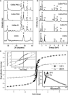
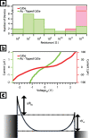
There has been significant interest in the development of multicomponent nanocrystals formed by the assembly of two or more different materials with control over size, shape, composition, and spatial orientation. In particular, the selective growth of metals on the tips of semiconductor nanorods and wires can act to couple the electrical and optical properties of semiconductors with the unique properties of various metals. Here, we outline our progress on the solution-phase synthesis of metal-semiconductor heterojunctions formed by the growth of Au, Pt, or other binary catalytic metal systems on metal (Cd, Pb, Cu)-chalcogenide nanostructures. We show the ability to grow the metal on various shapes (spherical, rods, hexagonal prisms, and wires). Furthermore, manipulating the composition of the metal nanoparticles is also shown, where PtNi and PtCo alloys are our main focus. The magnetic and electrical properties of the developed hybrid nanostructures are shown.
Keywords: Electrical and magnetic properties; Hybrid Nanocrystals; MOCVD; Nanowires; synthesis.
Figures


References
-
- Cozzoli PD, Pellegrino T, Manna L. Synthesis, properties and perspectives of hybrid nanocrystal structures. Chem Soc Rev. 2006;35:1195–208. - PubMed
-
- Peng X, Manna L, Yang W, Wickham J, Scher E, Kadavanich A, et al. Shape control of CdSe nanocrystals. Nature. 2000;404:59–61. - PubMed
-
- Subramanian V, Wolf EE, Kamat PV. Green emission to probe photoinduced charging events in ZnO-Au nanoparticles. Charge distribution and fermi-level equilibration. J Phys Chem B. 2003;107:7479–85.
-
- Pacholski C, Kornowski A, Weller H. Site-specific photodeposition of silver on ZnO nanorods. Angewandte Chemie Int Ed. 2004;43:4774–77. - PubMed
-
- Casavola M, Grillo V, Carlino E, Giannini C, Gozzo F, Fernandez E, et al. Topologically controlled growth of magnetic-metal-functionalized semiconductor oxide nanorods. Nano Lett. 2007;7:1386–95. - PubMed
LinkOut - more resources
Full Text Sources
Other Literature Sources
