Review
. 2010;10(10):8797-826.
doi: 10.3390/s101008797. Epub 2010 Sep 28.

Metal-insulator-semiconductor photodetectors

Affiliations
Review

Metal-insulator-semiconductor photodetectors

Chu-Hsuan Lin et al. Sensors (Basel). 2010.

Abstract

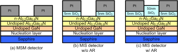
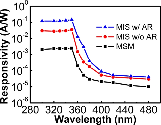
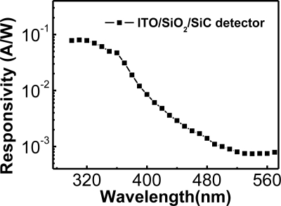
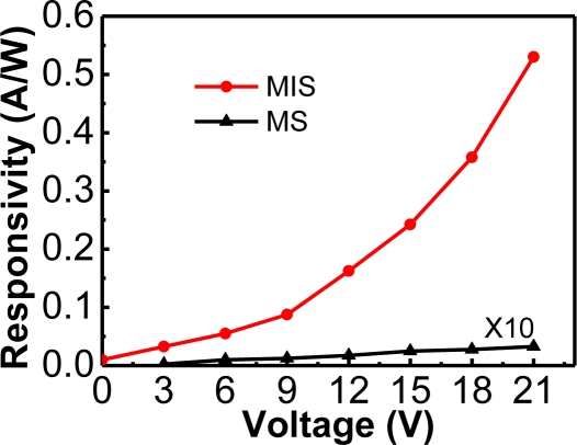
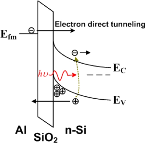
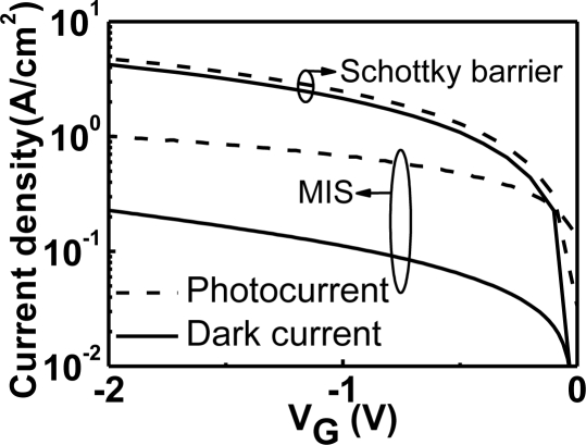
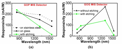
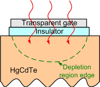
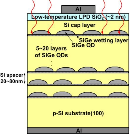
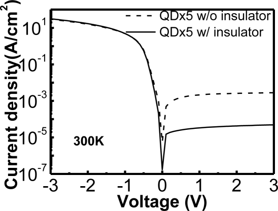
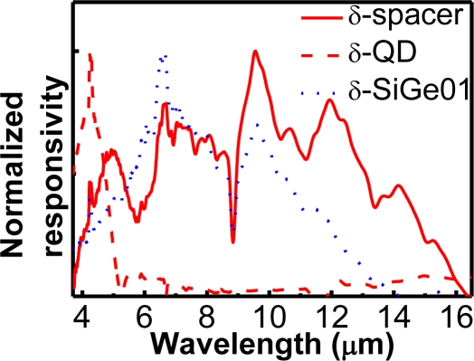
The major radiation of the sun can be roughly divided into three regions: ultraviolet, visible, and infrared light. Detection in these three regions is important to human beings. The metal-insulator-semiconductor photodetector, with a simpler process than the pn-junction photodetector and a lower dark current than the MSM photodetector, has been developed for light detection in these three regions. Ideal UV photodetectors with high UV-to-visible rejection ratio could be demonstrated with III-V metal-insulator-semiconductor UV photodetectors. The visible-light detection and near-infrared optical communications have been implemented with Si and Ge metal-insulator-semiconductor photodetectors. For mid- and long-wavelength infrared detection, metal-insulator-semiconductor SiGe/Si quantum dot infrared photodetectors have been developed, and the detection spectrum covers atmospheric transmission windows.

Keywords: MIS; metal-insulator-semiconductor; photodetector.


Figures

Figure 1.
Figure 1.
Gate tunneling current as a function of oxide thickness for various gate biases. In this example, the gate tunneling current is dominated by election tunneling from the conduction band of the vertical NMOS diode of an NMOSFET [7,8].
Figure 2.
Figure 2.
(a) The oxide voltage as a function of the gate voltage for a 3-nm-oxide NMOS with an NMOSFET transistor structure [8] and a 2.3 nm oxide NMOS without a transistor structure [9]; (b) Gate tunneling current density as a function of the gate voltage for a 2.9 nm oxide NMOS with an NMOSFET transistor structure [8] and a 2.3 nm oxide NMOS without a transistor structure [9].
Figure 3.
Figure 3.
The current mechanisms of an MIS diode (a) without light illumination; (b) with light illumination. A positive bias (inversion bias) is applied for this metal/insulator/p-type semiconductor example.
Figure 4.
Figure 4.
The schematic structures of metal-insulator-semiconductor photodetectors. (a) Light irradiates into the semiconductor from the unshadowed region when the metal is not transparent; (b) Light irradiates into the semiconductor passing through the transparent conducting oxide (TCO) or thin semi-transparent metal film.
Figure 5.
Figure 5.
Three different AlGaN/GaN structures: (a) MSM detector; (b) MIS detector without anti-reflection coating and (c) MIS detector with anti-reflection coating. The 50 nm thick SiO2 layer in (c) acts as both a passivation layer and anti-reflection coating. Reproduced from [23] with permission of Elsevier (2006).
Figure 6.
Figure 6.
Spectral responsivities of these three different photodetectors shown in Figure 5. The AlGaN/GaN MIS photodetector with AR coating has the highest UV-to-visible rejection ratio. Reproduced from [23] with permission of Elsevier (2006).
Figure 7.
Figure 7.
Spectral responsivity of the ITO/SiO2/SiC MIS photodetector. The UV (310 nm)-to-visible (500 nm) rejection ratio was ∼80. Reproduced from [31] with permission of Elsevier (2003).
Figure 8.
Figure 8.
Responsivity as a function of applied voltage for the Au/MgO/MgZnO MIS and Au/MgZnO MS photodetectors. The responsivity of the MIS detector increased exponentially, meanwhile the MS detector showed a linear behavior. Reproduced from [37] with permission of the American Chemical Society (2010).
Figure 9.
Figure 9.
The schematic mechanism of optical gain in the MIS photodetector. With the multiplication process, the external quantum efficiency of the MIS detector could achieve 200% at 21 V [37].
Figure 10.
Figure 10.
The schematic structure of a metal-filter (such as Ag) Si MIS UV photodetector. Incident photons were firstly selected by the gate, and then the remaining photons might be absorbed by Si to form the photocurrent.
Figure 11.
Figure 11.
Spectral responsivities of the Ag/SiO2/Si photodetectors with different thicknesses of Ag. The transmission of UV band at the ∼319 nm wavelength was due to the material property of Ag [40].
Figure 12.
Figure 12.
Dark current and photocurrents of the (a) Al/SiO2/p-Si MIS (NMOS) diode; (b) Al/SiO2/n-Si MIS (PMOS) diode. The inversion biases were positive and negative voltages for NMOS and PMOS photodetectors, respectively [9,50].
Figure 13.
Figure 13.
The schematic diagram of an Al/SiO2/n-Si MIS (PMOS) diode. The photo-generated holes contributed to the first plateau of the photocurrent and the electron direct tunneling contributed to the second plateau [50].
Figure 14.
Figure 14.
The schematic structure of a metal-insulator-semiconductor-insulator-metal photodetector. Both the anode and cathode electrodes were on the thin-insulator side.
Figure 15.
Figure 15.
The process flow of liquid phase deposition. The process can be operated at the temperature below 100 °C, and a thin (∼2 nm) SiO2 layer can be deposited on the Ge substrate [53].
Figure 16.
Figure 16.
Data communication system using a Ge MIS photodetector and a Ge MIS LED. The same MIS structure was used with different biases for different applications. The Ge MIS structure with an inversion bias acted as a detector, while it acted as an LED with an accumulation bias [55].
Figure 17.
Figure 17.
Modulation results of the data communication using a Ge MIS photodetector and a Ge MIS LED with a frequency of (a) 300 Kbit/sec; (b) 15 Mbit/sec. A delay time of ∼19 ns was observed in (b). Reprinted from [55] with permission of the American Institute of Physics (Copyright 2008).
Figure 18.
Figure 18.
The dark currents of Al/SiO2/n-Ge and Pt/SiO2/n-Ge photodetectors. The dark inversion current of the Pt gate device was smaller due to the suppression of electron tunneling from the metal to n-Ge [56].
Figure 19.
Figure 19.
The smart-cut process flow for demonstrating the GOI MIS photodetector. Thin films of 0.8–1.3 μm thick Ge were able to be transferred to the handle wafer.
Figure 20.
Figure 20.
The TEM photograph of the 0.8 μm thick-Ge GOI MIS photodetector. The low-temperature LPD SiO2 was formed on the thin-film Ge instead of the unstable GeO2.
Figure 21.
Figure 21.
Dark currents and photocurrents of the 1.3 μm thick-Ge GOI MIS and SB photodetectors. As compared with the SB detector, the MIS detector had a smaller dark current and a larger responsivity.
Figure 22.
Figure 22.
The responsivities of: (a) GOG MIS photodetectors; (b) GOP MIS photodetectors. Reprinted from [62,63] with permission of the American Institute of Physics (Copyright 2007 & 2009).
Figure 23.
Figure 23.
The typical structure of the HgCdTe MIS photodetectors. A pulse of voltage was applied to induce a deep-depletion region in the HgCdTe semiconductor for separation of photo-generated carriers.
Figure 24.
Figure 24.
The schematic structure of MIS SiGe/Si QDIPs. The low-temperature LPD SiO2 layer was adopted in order to avoid the strain relaxation and interdiffusion between Si and Ge.
Figure 25.
Figure 25.
Dark currents of five-period SiGe/Si QDIPs with and without an insulator layer between the metal and semiconductor. A QD sample with the insulator layer indeed can reduce the dark inversion current. Reproduced from [80] with permission of Elsevier (2006).
Figure 26.
Figure 26.
Spectral responses of the MIS SiGe/Si quantum dot (well) infrared photodetectors at 15 K. For the spacer sample, the detection regions of 3.7–6 and 6–16 μm corresponded to the LH1-to-LH3 transition in QDs, and intraband transitions in the boron doping wells, respectively [83].

References

    1. Monroy E, Omnès F, Calle F. Wide-Bandgap Semiconductor Ultraviolet Photodetectors. Semicond. Sci. Technol. 2003;18:R33–R51.
    1. Park JS, Lin TL, Jones EW, Castillo HMD, Gunapala SD. Long-Wavelength Stacked SiGe/Si Heterojunction Internal Photoemission Infrared Detectors Using Multiple SiGe/Si Layers. Appl. Phys. Lett. 1994;64:2370–2372.
    1. Rogalski A. Quantum Well Photoconductors in Infrared Detector Technology. J. Appl. Phys. 2003;93:4355–4391.
    1. Kasper E, Oehme M. High Speed Germanium Detectors on Si. Phys. Stat. Sol. C. 2008;5:3144–3149.
    1. Brennan KF, Haralson J, Parks JW, Salem A. Review of Reliability Issues of Metal-Semiconductor-Metal and Avalanche Photodiode Photonic Detectors. Microelectron. Reliab. 1999;39:1873–1883.

LinkOut - more resources