. 2011;11(9):9009-32.
doi: 10.3390/s110909009. Epub 2011 Sep 21.

A programmable plug & play sensor interface for WSN applications

Affiliations

A programmable plug & play sensor interface for WSN applications

Sergio D Vera et al. Sensors (Basel). 2011.

Abstract

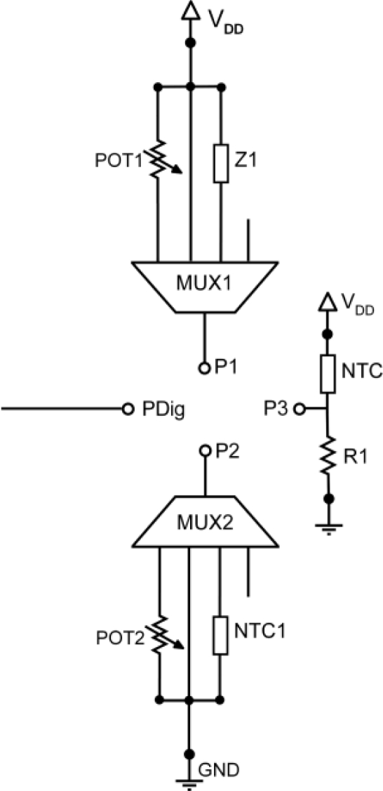
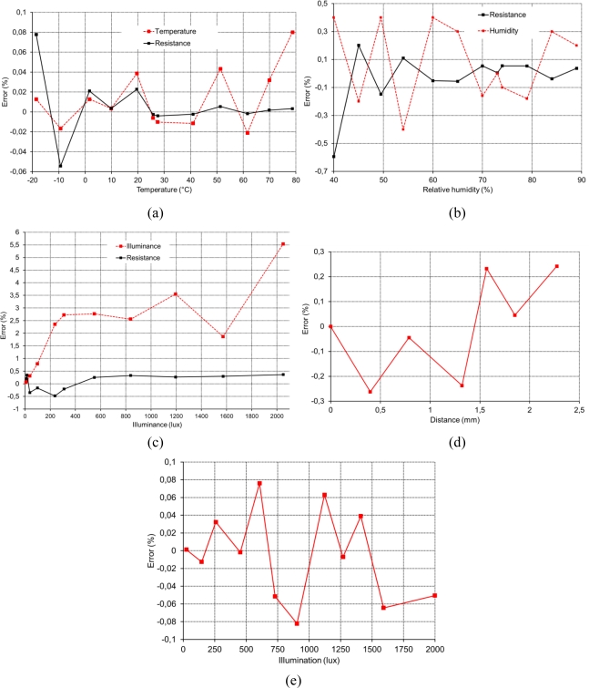
Cost reduction in wireless sensor networks (WSN) becomes a priority when extending their application to fields where a great number of sensors is needed, such as habitat monitoring, precision agriculture or diffuse greenhouse emission measurement. In these cases, the use of smart sensors is expensive, consequently requiring the use of low-cost sensors. The solution to convert such generic low-cost sensors into intelligent ones leads to the implementation of a versatile system with enhanced processing and storage capabilities to attain a plug and play electronic interface able to adapt to all the sensors used. This paper focuses on this issue and presents a low-voltage plug & play reprogrammable interface capable of adapting to different sensor types and achieving an optimum reading performance for every sensor. The proposed interface, which includes both electronic and software elements so that it can be easily integrated in WSN nodes, is described and experimental test results to validate its performance are given.

Keywords: TEDS; embedded microcontroller; plug & play; sensor interface; smart sensors; wireless sensor networks.


Figures

Figure 1.
Figure 1.
Complete scheme diagram of the proposed sensor interface and communications.
Figure 2.
Figure 2.
Sensor platform.
Figure 3.
Figure 3.
Amplification System.
Figure 4.
Figure 4.
STIM μC’s RAM memory with NTC information.
Figure 5.
Figure 5.
Basic STIM μC operations flow for (left) first connection and (right) measurement request.
Figure 6.
Figure 6.
Chronogram of a first plug and measurement of the STIM into the sensor node.
Figure 7.
Figure 7.
Direct Counting Method timing diagram.
Figure 8.
Figure 8.
Photograph of the sensor interface (dimensions: 76 × 46 mm).
Figure 9.
Figure 9.
STIM power levels.
Figure 10.
Figure 10.
NTC behavior: (a) Experimental characterization; (b) Conditioning interface scheme; (c) Resistive divider output voltage, function of the corresponding sensed temperature; and (d) Conditioned output sensor range fit to a common 0–VDD range (x) and VFC output (o).
Figure 11.
Figure 11.
STIM μC’s RAM memory with RH sensor information.
Figure 12.
Figure 12.
Humidity sensor behavior at 26 °C: (a) Experimental characterization; (b) Conditioning interface scheme, (c) Resistive divider output voltage, function of the corresponding sensed temperature; and (d) Conditioned output sensor range fit to a common 0–VDD range (x) and VFC output (o).
Figure 12.
Figure 12.
Humidity sensor behavior at 26 °C: (a) Experimental characterization; (b) Conditioning interface scheme, (c) Resistive divider output voltage, function of the corresponding sensed temperature; and (d) Conditioned output sensor range fit to a common 0–VDD range (x) and VFC output (o).
Figure 13.
Figure 13.
LDR behavior (x) and output voltage obtained from the master μC after the application of the DCM to the frequency-coded signal provided by the STIM (o).
Figure 14.
Figure 14.
Hall sensor behavior (x) and output voltage obtained from the master μC after the application of the DCM to the frequency-coded signal provided by the STIM (o).
Figure 15.
Figure 15.
Photodiode output (x) and output voltage obtained from the master μC after the application of the DCM to the frequency-coded signal provided by the STIM (o).
Figure 16.
Figure 16.
Full scale errors associated with the interface electronics for (a) NTC; (b) RH sensor; (c) LDR; (d) linear Hall sensor and (e) photodiode.

References

    1. Krishnamachari B. Networking Wireless Sensors. Cambridge University Press; New York, NY, USA: 2005.
    1. Bissi L, Placidi P, Scorzoni A, Elmi I, Zampolli S. Environmental monitoring system compliant with the IEEE 1451 standard and featuring a simplified transducer interface. Sens. Actuat. A Phys. 2007;137:175–184.
    1. Pal S, Rakshit A. Development of network capable smart transducer interface for traditional sensors and actuators. Sens. Actuat. A Phys. 2004;112:381–387.
    1. Mattoli V, Mondini A, Mazzolai B, Ferri G, Dario P. A universal intelligent system-on-chip based sensor interface. Sensors. 2010;10:7716–7747. - PMC - PubMed
    1. Kirianaki NV, Yurish SY, Shpak NO, Deynega VP. Data Acquisition and Signal Processing for Smart Sensors. John Wiley & Sons; Chichester, UK: 2002.

Publication types

LinkOut - more resources