Review
. 2010;10(6):5469-502.
doi: 10.3390/s100605469. Epub 2010 Jun 1.

Metal oxide semi-conductor gas sensors in environmental monitoring

Affiliations
Review

Metal oxide semi-conductor gas sensors in environmental monitoring

George F Fine et al. Sensors (Basel). 2010.

Abstract

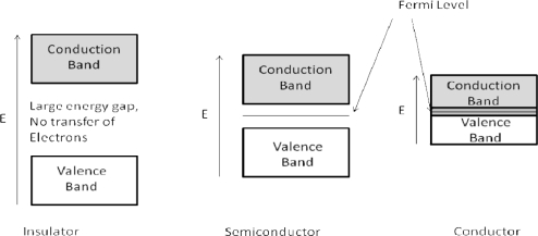
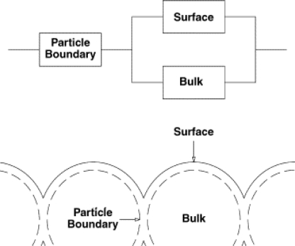
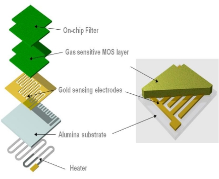
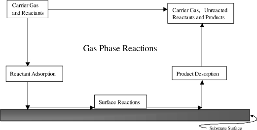
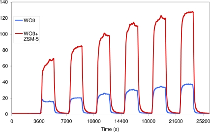
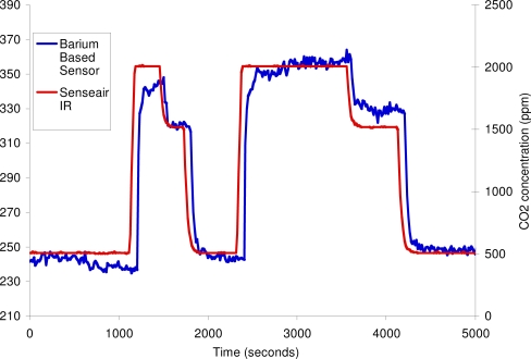
Metal oxide semiconductor gas sensors are utilised in a variety of different roles and industries. They are relatively inexpensive compared to other sensing technologies, robust, lightweight, long lasting and benefit from high material sensitivity and quick response times. They have been used extensively to measure and monitor trace amounts of environmentally important gases such as carbon monoxide and nitrogen dioxide. In this review the nature of the gas response and how it is fundamentally linked to surface structure is explored. Synthetic routes to metal oxide semiconductor gas sensors are also discussed and related to their affect on surface structure. An overview of important contributions and recent advances are discussed for the use of metal oxide semiconductor sensors for the detection of a variety of gases--CO, NO(x), NH(3) and the particularly challenging case of CO(2). Finally a description of recent advances in work completed at University College London is presented including the use of selective zeolites layers, new perovskite type materials and an innovative chemical vapour deposition approach to film deposition.

Keywords: environmental monitoring; metal oxides; semiconductor; zeolites.


Figures

Figure 1.
Figure 1.
Schematic band diagrams of an insulator, semi-conductor and conductor—Note the small gap in the semiconductor, where electrons with sufficient energy can cross and the overlapping of the bands in the conductor.
Figure 2.
Figure 2.
Demonstrating the structure of the materials, and the positions of the surface, bulk and particle boundary. Figure adapted with permission from Naisbitt et al. [13]. The model assumes the gas sensitivities of the surface and particle boundary are the same.
Figure 3.
Figure 3.
Demonstrating the production of a gas sensitive film on a sensor substrate (diagram courtesy of Capteur Sensors and Analysers).
Figure 4.
Figure 4.
A basic outline of the CVD method, depositing a film on to the substrate surface. Figure adapted with permission from [22].
Figure 5.
Figure 5.
Demonstrating the spray pyrolysis technique for depositing thin films. Figure adapted with permission from Tischner et al. [30].
Figure 6.
Figure 6.
Schematic of the PVD process, adapted with permission from Kanu et al. [19].
Figure 7.
Figure 7.
Showing the sensor response to varying concentrations of carbon monoxide for both a SnO2 sensor and an IR gas analyser. Figure adapted with permission from [45].
Figure 8.
Figure 8.
The effect of grain size on the size of response to the carbon monoxide target gas. Figure adapted with permission from [46].
Figure 9.
Figure 9.
Demonstrating the response of the sensor to humidity. Note the decrease in baseline response over time and successive introductions. Figure adapted with permission from [30].
Figure 10.
Figure 10.
The response of rutile film to carbon monoxide at various temperatures. Figure adapted with permission from [48].
Figure 11.
Figure 11.
A graph depicting the steady increase in CO2 concentrations since 1958 at the Mauna Loa Observatory. Figure adapted from [52].
Figure 12.
Figure 12.
response of the SnO2 film developed by Hoefer et al. to CO2 gas in synthetic air at 270 °C. Figure adapted with permission from [56].
Figure 13.
Figure 13.
The responsivity change of the Lanthanum film to carbon dioxide upon increasing concentration (temperature unreported). Figure adapted with permissions from [57].
Figure 14.
Figure 14.
The effect of varying CO2 concentration on the signal of the BaTiO3 sensing material (note the baseline increase over time). Figure adapted with permission from [58].
Figure 15.
Figure 15.
Results demonstrating the effect in changing La concentration on the responsivity of the SnO2 film, also showing poor discrimination between carbon monoxide and carbon dioxide. Figure adapted with permission from [59].
Figure 16.
Figure 16.
The variation in resistance according to WO3 crystallite size for; □ air, and ▪5 ppm NO2 in air at 300 °C. Figure adapted with permission from [65].
Figure 17.
Figure 17.
Demonstrating the effect of firing temperature on the responsivity of the WO3 film. Figure adapted with permission from [67].
Figure 18.
Figure 18.
The effect of doping the material with various oxides on the responsivity of SnO2 to N2O gas. Figure adapted with permission from [70].
Figure 19.
Figure 19.
Graph comparing the responses of chemiluminescence and semiconductor sensors. Measurements were simultaneous and made every minute. X-axis indicates hours since experiment start and y-axis ppb concentration of NO2. Figure adapted with permission from [73].
Figure 20.
Figure 20.
Left, The responses (as %) of pure ZnO thick films fired at varying temperatures to 1,000 ppm of ammonia. Right, showing the optimum operating temperature for ZnO films for sensing 1,000 ppm ammonia with RuO2 doping. Figure adapted with permission from [78].
Figure 21.
Figure 21.
Schematic of sensor fabrication, Left a standard screen-printed sensor, Right a sensor modified with a zeolites over-layer.
Figure 22.
Figure 22.
Gas responses of tungsten oxide and zeolites modified tungsten oxide sensors to 100, 120, 140, 160, 180, 200 ppb NO2 in dry air at 350 °C.
Figure 23.
Figure 23.
Comparison of CO2 Sensor Technologies: Commercial Senseair Infra-red device versus a barium based metal oxide semiconductor sensor developed at UCL. CO2 concentration indicated by the K30 is plotted on right hand axis and the UCL sensor response is on left hand axis, showing a change in resistance in the MOhm region.
Figure 24.
Figure 24.
(Left) Schematic illustrates the CVD reactor design used in the production of sensors using ElFi CVD. (Right) Example morphology of vanadium dioxide thin films grown on sensor substrates from the ElFi CVD reaction of vanadyl acetylacetonate at 525 °C with an applied AC electric field.

Similar articles

Cited by

References

    1. Seiyama T., Kato A., Fujiishi K., Nagatani M. A new detector for gaseous components using semiconductive thin films. Anal. Chem. 1962;34:1502–1503.
    1. Elmi I., Zampolli S., Cozzani E., Mancarella F., Cardinali G.C. Development of ultra-low-power consumption MOX sensors with ppb-level VOC detection capabilities for emerging applications. Sens. Actuat. B-Chem. 2008;135:342–351.
    1. Guo Y., Zhang X.W., Han G.R. Investigation of structure and properties of N-doped TiO2 thin films grown by APCVD. Mater. Sci. Eng.: B. 2006;135:83–87.
    1. Gurlo A., Bârsan N., Ivanovskaya M., Weimar U., Göpel W. In2O3 and MoO3–In2O3 thin film semiconductor sensors: interaction with NO2 and O3. Sens. Actuat. B-Chem. 1998;47:92–99.
    1. Kida T., Nishiyama A., Yuasa M., Shimanoe K., Yamazoe N. Highly sensitive NO2 sensors using lamellar-structured WO3 particles prepared by an acidification method. Sens. Actuat. B-Chem. 2009;135:568–574.

LinkOut - more resources